Continue to Site

Welcome to EDAboard.com

Welcome to our site! EDAboard.com is an international Electronics Discussion Forum focused on EDA software, circuits, schematics, books, theory, papers, asic, pld, 8051, DSP, Network, RF, Analog Design, PCB, Service Manuals... and a whole lot more! To participate you need to register. Registration is free. Click here to register now.

problem on the matching networks

Status
Not open for further replies.

lsfeng

Junior Member level 1
Joined
Oct 5, 2007
Messages
19
Helped
0
Reputation
0
Reaction score
0
Trophy points
1,281
Activity points
1,429
hello ,everyone
I am a begainer on the matching network,and come about some questions as follows:
1 the pi-match could be seen as two L-match's combination,so the resonating
frequency must be the same ?
2 if the circuit has good match on the unexpection frequency , so the Q of the
circuit is too low or not?
3 the matches I have done is on the single frequency,so how to make a wideband
match using the pi network or other methord?

that 's all , thank you:D


first of all, your questions were not quite clear. anyway, I would like to answer them:

1. for matching, you don't need resonance. Moreover, if you want to calculate resonant frequency of each L-section, they may not be the same. Please take a look at this tutorial

**broken link removed**

2. Low Q refers to higher bandwidth. If you see a high BW matching you know the Q is low for that circuit.

3. You need cascading to get wideband match. However, you have limit (Bode-Fano criterion). If possible try to find the book of Pozar "Microwave Engineering". Matching is very well explained there.
 

    lsfeng

    Points: 2
    Helpful Answer Positive Rating
When you think of a Pi-network being the same as 2 L-networks do you mean
a network with 4 or 3 components (if they are lumped elements in a schematic)?

2 L-networks would be 4 components and a Pi-network will have 3.

Also at high frequencies you have to remember that as you add components
in your matching network you will introduce length which will change the networks
overall impedance. Look up "Stub Tunning", and "1/4 wave transforms" to get
an understanding of the wavelength to impedance relations (Pozar is good).
 

    lsfeng

    Points: 2
    Helpful Answer Positive Rating
first of all ,thank you for your replies,
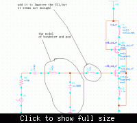
maybe ,I don't express my question very clear ,now I am designing a common source LNA ,and the S11 is very bad(-7,8dB),I want to make it better by improve the
input match network.Considering the effect of bondwire and pad of input signal,the quetion seems more difficult to me,the schematic is as follows ,how can I make an input match network to achieve both a good S11 and NF at the same time ,thank you!

ps: the book " microwave egineer" is usefull for RF designing?
 

For the input match of an LNA, there's a well known trade off between noise figure and s11 (gain). You can't simultaneously optimize for both. You can take a look at "The Design of CMOS Radio-Frequency Integrated Circuits" by Thomas Lee. This concept is explained pretty well in its LNA chapter.
 

thank u ,I have read that book many times ,and its LNA chapter is not considering the effect of bondwire and pad ,and the working condition is ideal,but mine is not. my circuit is working on 3-5GHz, so the imput match should be wideband!
how do i make it?
 

First of all, you need to define how much S11 (return loss) is acceptable for your design. Then you have two different options:

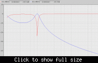
From your graph, you get minimum S11 (return loss) around -24 dB. If you need only -15 dB (as an example) you can use overcoupling, not critical coupling. Then see how much bandwidth you achieve. [overcoupling means S11 does not pass through the center of the chart, please look at Pozar book about the definitions]. If you don't get enough bandwidth you use multiple stages as I told earlier.
 

Status
Not open for further replies.

Similar threads

Part and Inventory Search

Welcome to EDABoard.com

Sponsor

Back
Top