Continue to Site

Welcome to EDAboard.com

Welcome to our site! EDAboard.com is an international Electronics Discussion Forum focused on EDA software, circuits, schematics, books, theory, papers, asic, pld, 8051, DSP, Network, RF, Analog Design, PCB, Service Manuals... and a whole lot more! To participate you need to register. Registration is free. Click here to register now.

problem in Dual Active Bridge(LT-spice implementation)

Status
Not open for further replies.

Fayaz143

Newbie level 6
Joined
Mar 15, 2021
Messages
14
Helped
1
Reputation
2
Reaction score
0
Trophy points
1
Activity points
144
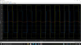
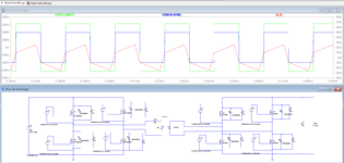
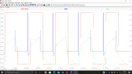
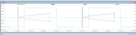
hello, I am trying to simulate Dual Active Bridge converter in LT spice. I have try simulation in Matlab Simulink where I am getting the desired phase shift. But i am simulating in LT spice, I am not able to produce the phase shift b/w the primary and secondary of the coupled inductor transformer.

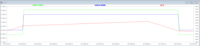
As the power and voltage level linking the primary and the secondary of the transformer are different, I should choose different Mosfet switches for the each bridge and does these Mosfet have Parasitic capacitance parallel from drain to source. Or else I should place a capacitor in parallel to have the operation of soft switching. Any suggestion how to obtain the phase shift and Zero voltage switching.
 

Attachments

  • Screenshot (486).png
    Screenshot (486).png
    112.5 KB · Views: 602
  • Screenshot (527).png
    Screenshot (527).png
    68.8 KB · Views: 844

looking at the waveforms - you already have it - try zooming in on the edges ...
--- Updated ---

Just a note - the rail voltage do not match the device ratings - you should correct that either by different devices or by scaling the input bus etc
 

looking at the waveforms - you already have it - try zooming in on the edges ...
--- Updated ---

Just a note - the rail voltage do not match the device ratings - you should correct that either by different devices or by scaling the input bus etc
@Easy peasy Thanks for the advice. I have zoomed it,But both the voltages are overlaping
 

Yes as Easy Peasy said it looks like your already ZVS'ing. Your waveforms look like those of a Phase shift full bridge.
To check if you are ZVS'ing.....just "scope" the drain source of a fet.......and also display the current in the FET........you should see the FET DS voltage go to near zero before current in the drain to source direction starts flowing in it.

Pretty much all resonant switching converters are the same, in that they get conduction in their intrinsic diode just before they get switched ON....easy for you to check in the sim.
 
I don't expect ZVS with no dead time between gate voltage pulses. You get even shoot-through with the actual parameters.
Don't looks like you put much effort in designing the drive waveforms.
--- Updated ---

I am not able to produce the phase shift b/w the primary and secondary of the coupled inductor transformer.
Why, particularly?
 
Good point, yes, please show us a scope shot of the current in one of the FETs...over say 6 switching cycles.
 
Thank you all for the response. How to scope Vds and Ids of FET in LT-spice. I am only able to plot drain current which is Id(M1).
 

Attachments

  • Screenshot (534).png
    Screenshot (534).png
    29.7 KB · Views: 193
  • Screenshot (535).png
    Screenshot (535).png
    116.2 KB · Views: 189

for current in a branch, press down the ALT key, then you click on the branch where you want to see the current.
For any voltage between two nodes, simply click one node, hold on the click and move over to the other node, then click on that.
Attached is a beginners guide to LTspice
 

Attachments

  • LTspice _Quick Start Guide.zip
    4.4 KB · Views: 183
I am only able plot Id(M1), Is(M1), Ig(M1) but How to plot the Ids(M1) and Vds(M1) of the FETs so that I can check whether ZVS operation is occurring or not
I have attached the file of Dual active bridge below. if you can scope Ids(M1), Vds(M1) for me that would be a great help. @Easy peasy, @treez
 

Attachments

  • Screenshot (537).png
    Screenshot (537).png
    26.8 KB · Views: 138
  • DAB1.zip
    2 KB · Views: 220

Id(M1) will be the same as Ids(M1) (as near as dammit). -Apart from the drain gate charge current.
If you really want to know IDS exactly...then you know Kirchoff's Law....and you know Ig, Is and Id....so you shoudl be able to get Ids(M1).
...Do it by putting an expression in the waveform window of Id(M1) - Ig(M1). That equals Ids(M1)
.Mind you watch the signs.....I think current into the terminal is positive.
--- Updated ---

OK, attached is your DAB sim but ive edited it.
I had to reduce vin to 780v as the diodes are breaking over at 800v (even on the sim) and conducting big spikes in reverse direction (they arre only 800v rated)
Also, i have interleaved your gate drive signals so they dont give so much shoot thru.
Also, i took off the DS capacitors, as they werent doing anything good.

Also, i changed your didoes and fets up from the 100v ones you had in there.

It seems to be working pretty well now. I suppose the next bit would be to do the duty cycle modulation via phase shifting the diagonal legs with respect to each other.
--- Updated ---

I must admit it seems like getting something for nothing....a bidirectional high power converter with just a sizeable inductor added in series with the primary.
--- Updated ---

woops sorry, here is the correction, i previously mis-phased your synchronous fets...here now corrected
--- Updated ---

Aaaaaah!...not having a good day today...accidentally used the primary on time for the secondary aswell...here it is corrected..."DAB4_edited"
--- Updated ---

..Actually, with "DAB2_edited" i put in a typo by mistake, and it ended up phase shifting the secondary synch fets with respect to the primary ones, and yet the output power was a lot more and there appeared to be no bad shoot thru.
 

Attachments

  • DAB2_edited.zip
    2.2 KB · Views: 128
  • DAB2_edited.pdf
    162.5 KB · Views: 173
  • DAB3_edited.pdf
    162.5 KB · Views: 114
  • DAB3_edited.zip
    2.2 KB · Views: 103
  • DAB4_edited.pdf
    162.4 KB · Views: 203
  • DAB4_edited.zip
    2.2 KB · Views: 237
Last edited by a moderator:
Thanks @treez for you support and time.

How can I further improve. Where am I going wrong? Are the pulse generator for secondary bridge are wrong? How get the phase shift from primary to Secondary?
 

How can I further improve. Where am I going wrong? Are the pulse generator for secondary bridge are wrong? How get the phase shift from primary to Secondary?
The fault in post #1 is looking at the wrong voltages. Primary and secondary voltage of an ideal transformer are always in phase. Instead you want to look at the primary and secondary bridge output voltage, respectively voltage at both sides of the series inductor. The current waveform reveals that the circuit is operating with phase shift, by the way.

Second fault is driving the transistors without dead time. The point has been verbosely addressed in the edited circuits by treez. To get the intended behaviour in the original circuit, it's sufficient to reduce ton of all drivers from 10 µs to 9 µs, keeping all other parameters, also the 10 nF capacitors.

1623771446335.png
 
Last edited:

The fault in post #1 is looking at the wrong voltages. Primary and secondary voltage of an ideal transformer are always in phase. Instead you want to look at the primary and secondary bridge output voltage, respectively voltage at both sides of the series inductor. The current waveform reveals that the circuit is operating with phase shift, by the way.

Second fault is driving the transistors without dead time. The point has been verbosely addressed in the edited circuits by treez. To get the intended behaviour in the original circuit, it's sufficient to reduce ton of all drivers from 10 µs to 9 µs, keeping all other parameters, also the 10 nF capacitors.

View attachment 170192
My bad, all this time I was looking at the ideal transformer voltage waveform and wondering why there isn't a phase shift. Thank you very much for the help.
 

Status
Not open for further replies.

Similar threads

Part and Inventory Search

Welcome to EDABoard.com

Sponsor

Back
Top