Continue to Site

Welcome to EDAboard.com

Welcome to our site! EDAboard.com is an international Electronics Discussion Forum focused on EDA software, circuits, schematics, books, theory, papers, asic, pld, 8051, DSP, Network, RF, Analog Design, PCB, Service Manuals... and a whole lot more! To participate you need to register. Registration is free. Click here to register now.

[SOLVED] Problem In Component Placement in Orcad Layout Plus 16.0

Status
Not open for further replies.

gatzrulz

Newbie level 5
Joined
Oct 20, 2009
Messages
8
Helped
0
Reputation
0
Reaction score
0
Trophy points
1,281
Location
India
Activity points
1,349
Hi Frnds,

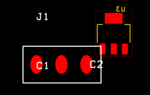
Im designing a PCB with Orcad Capture for Circuit and Orcad Layout Plus for PCB Designing. i have created a SMD Component using Library Manager and the photo is attached.

It was done using SSTOP, TOP, SPTOP, SMTOP.

Question No 1
Can i use the Opposite command by right clicking on the component, to use it at the bottom of the PCB.

Question No 2
When i place a SMD Component on TOP layer i couldnt able to place another component on the BOTTOM layer just exactly back side to the component placed on TOP Layer. Its showing a Unable to Clear or Verify DRC.

Thanks In Advance.
 

Attachments

  • SMD Component.PNG
    SMD Component.PNG
    23.5 KB · Views: 137

Question No 1
Can i use the Opposite command by right clicking on the component, to use it at the bottom of the PCB.

you just need to select bottom layer while placing component in bottom.you can select bottom layer using numeric 2 key.and then it automatically rotate the component.

Question No 2
When i place a SMD Component on TOP layer i couldnt able to place another component on the BOTTOM layer just exactly back side to the component placed on TOP Layer. Its showing a Unable to Clear or Verify DRC.

while doing lay out just turn off DRC rule check tool.after completion you can check the DRC rules not all just few as required by your application.
 
Hi,

Thanks for your support.

The attached image is showing a overlapping of component. but this im placing one component in top layer and the other in bottom layer. practically speaking error should not come. so im eager to know the reason for error. it says "unable to clear DRC" and its not allowing to place without disabling the DRC. is there any way avoid this error other than disabling the DRC.

also in some designs im getting "Insufficient clearence on plane layer". but no way i can increase the gap between the pads. i used Pad size 60, SMT & SMB 65, drill size 30 or 35. im using 2 side pcb . so only top and bottom layers im using. no plane ,gnd & inner layers are used.

Thanks In Advance.
 

Attachments

  • SMD.PNG
    SMD.PNG
    6 KB · Views: 147

you can not place a through whole component below the smd part.That is way you are getting error. and you can change the clearance parameter also if you have PCB size problem.

As per image your components looks overlapped.
 

Thank You. you are right when im placing a SMD component in the same X,Y co ordinates respectively one at bottom and the other at the top im not getting any error.

But im just wondering how to change the clearance parameter. at any point i cant able to change the pad width & height and the pitch between pins.
 

you can change the pad height and width using the padstack tool in the TOOL option in menu bar.
For clearance you can do with the Global Spacing setting under the Option settings.
 

Status
Not open for further replies.

Part and Inventory Search

Welcome to EDABoard.com

Sponsor

Back
Top