heena123
Banned
hi,
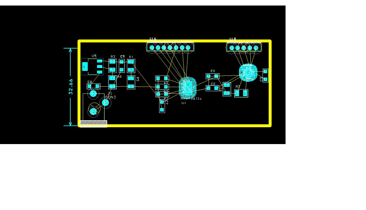
I am design one layout for my project in this layout all component is SMD package type,
I am also given same footprint to it ,
but still when i completed my component placement it gave me
ERROR 136 Something.
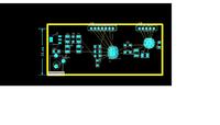
I also give a snap shoot of that error was occurred
Please reply me for this
Regards,
Heena
I am design one layout for my project in this layout all component is SMD package type,
I am also given same footprint to it ,
but still when i completed my component placement it gave me
ERROR 136 Something.
I also give a snap shoot of that error was occurred
Please reply me for this
Regards,
Heena