Continue to Site

Welcome to EDAboard.com

Welcome to our site! EDAboard.com is an international Electronics Discussion Forum focused on EDA software, circuits, schematics, books, theory, papers, asic, pld, 8051, DSP, Network, RF, Analog Design, PCB, Service Manuals... and a whole lot more! To participate you need to register. Registration is free. Click here to register now.

Problem finding out the Vout for PMOS and NMOS

Status
Not open for further replies.

melryin

Newbie level 4
Joined
Aug 2, 2007
Messages
7
Helped
1
Reputation
2
Reaction score
1
Trophy points
1,283
Activity points
1,328
I have problem to find out the Vout for the circuits on the attachment. Can anyone please teach me how to identify it? Your help is very much appreciated!!!
 

Can u please draw the diagram vertically and clearly so that i can understand ur quetion clearly

take care
 

the output of the first circuit is 3.6V and that of the second circuit is 4.3V....
 

A.Anand Srinivasan said:
the output of the first circuit is 3.6V and that of the second circuit is 4.3V....
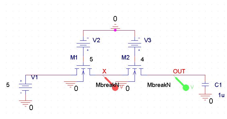
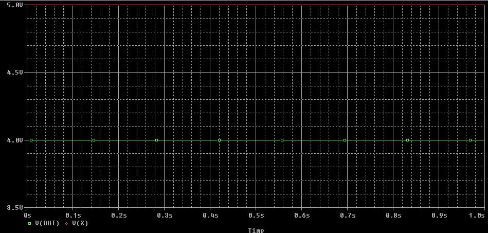
thanks!! but I'm not very sure why the 1st one is not 3.3 since Vout = Vdd - Vtn?

Sorry, I'm a bit dumb on MOS, can you pls explain to me how you get the answer? So I can learn more from you!

Thank you so much for your help!!!:D
 

rajanarender_suram said:
i think 1st one is 3.3V and second one is certainly 5V
i was thinking, the 1st one is Vout=Vdd-Vtn regardless of what is before that. and the second one, since Vg is less than Vd-Vtp, so Vout = Vin, am I right to think so???

Thank you so much guys!!!
 

for 1st one the out put is

Vout=vin for vg-vin>vth
vout =vg-vth for vg-vin<vth

this is what i know
 

for the first one Vdd is made 4.3V by the FET before it and hence the output is 4.3-.7V = 3.6V.... second one it is Vdd-Vt=4.3V...
 

No no no, this is pass transistor logic...
For the first circuit Vout=4V, for the second Vout=5V...
 

the_edge said:
No no no, this is pass transistor logic...
For the first circuit Vout=4V, for the second Vout=5V...
Can you pls explain a bit what is pass transistor? I saw some examples on the pass transistors which are similar to these. BUT i'm not clear what is pass transistor.

Thank you!
 

This is pass-transistor logic...
12_1186414841.jpg

The idea is that both transistor are ON at the same time...
Your example is just with one transistor.
I will ask you to tell me where is drain and source of both transistor... I will not answer it till tomorow, so please think about it...
 

First one is certainly 3.3 V

the second one is a perfect example showing that a pmos is "strong one"

The o/p must be 5 v

Remember for both pmos and nmos Vt has a relationship with only Vgs for the device to be conducting ,since in the second circuit the capacitor is placed at the drain of pmos and the condition for pmos to be on Vsg≥|Vt| which is already satisfied the capacitor is charged to complete 5v.
 

the_edge said:
This is pass-transistor logic...
12_1186414841.jpg

The idea is that both transistor are ON at the same time...
Your example is just with one transistor.
I will ask you to tell me where is drain and source of both transistor... I will not answer it till tomorow, so please think about it...
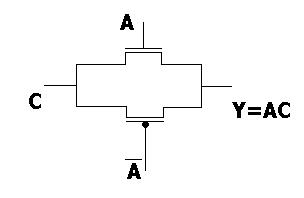
Do you mean, telling you where is drain and source for the picture you have posted?

If so, I think point C is the source for both transistor. Am I right???
 

Status
Not open for further replies.

Part and Inventory Search

Welcome to EDABoard.com

Sponsor

Back
Top