shavarna.jiit
Newbie level 4
- Joined
- Jun 29, 2010
- Messages
- 5
- Helped
- 0
- Reputation
- 0
- Reaction score
- 0
- Trophy points
- 1,281
- Location
- United States
- Activity points
- 1,320
Hello,
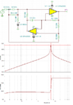
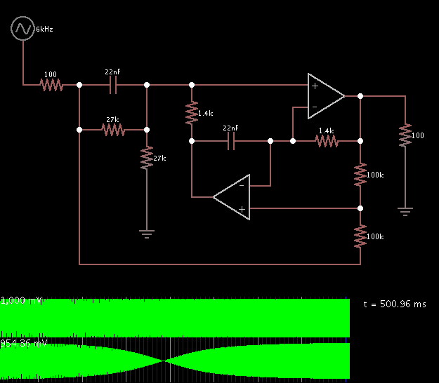
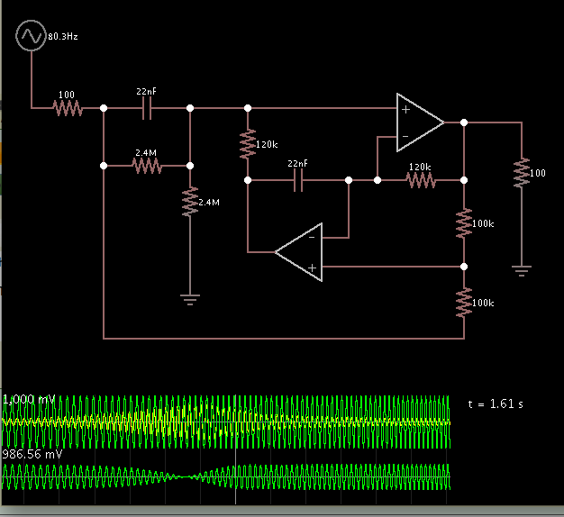
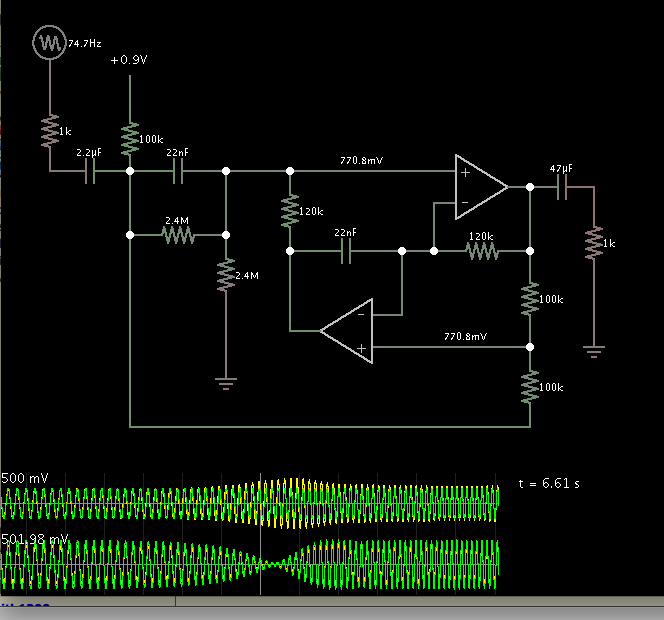
I am trying to design a Fliege Notch Filter at 5.6 KHz for design of neuronal signal acquisition system. I am using op-amp OPA2333 with single supply. However the output to the circuit amazed me because it acts like an narrow band pass filter instead of notch filter.
I really appreciate if someone could point out the error. Attached is the simulation Circuit and Output.
I have done this design on the basis of basic steps mentioned in https://www.ti.com/lit/an/sloa093/sloa093.pdf Page 9