Continue to Site

Welcome to EDAboard.com

Welcome to our site! EDAboard.com is an international Electronics Discussion Forum focused on EDA software, circuits, schematics, books, theory, papers, asic, pld, 8051, DSP, Network, RF, Analog Design, PCB, Service Manuals... and a whole lot more! To participate you need to register. Registration is free. Click here to register now.

[SOLVED] Problem about the Power Efficiency of EM simulation and Schematic simulation for 2.45 GHz Energy Harvesting

Status
Not open for further replies.

erihengz

Newbie
Joined
Jul 11, 2021
Messages
3
Helped
0
Reputation
0
Reaction score
1
Trophy points
3
Activity points
42
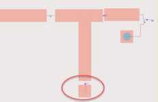
Hi, currently i am designing a 2.45ghz energy harvesting system. The below part is my rectifier schematic.
1626236653236.png


The matching is tuned and the S-parameter hits below -10 dB, which is shown as below.
1626236763181.png


It seems good and the result from the schematic is what I desired to have.

The problem is when I moved my schematic to layout and did EM simulation. The result is completely mismatch and the effciency is very low.
1626236898967.png

1626237051066.png


1626237191553.png

The S11-response probably can be optimzed again to hit 2.45ghz. But I have no idea why the power conversion efficiency is so low.

BTW, I just approached ADS for no longer time. I hope that anyone can help explain to me and help me with this.
 
The S11-response probably can be optimzed again to hit 2.45ghz. But I have no idea why the power conversion efficiency is so low.
You understand that both figures are closely related? To get an idea about possible efficiency, you'd measure it at the actual resonance frequency of about 2.35 GHz. You should be able to tune the geometry for 2.45 GHz resonance.

Problem is however the designed small bandwidth, effectively useless for a real world matching circuit that shall work without tuning.
 
Actually, I don't know what the problem is but I can say a bit about this situation.
As known, the results of the EM simulation can differ from the schematic results enormously. As I learnt from my professor, the most accurate and consolidated way to obtain compatible results with schematic and EM simulations is to proceed step by step. In other words, you shouldn't run an EM simulation after the overall circuit is built. Just take a part of the circuit by starting from the beginning, check schematic results and then, check EM results too. See the compatibility between them. Afterwards, go for adding the next few elements and do the same steps. Whenever the results go unexpected or bad, it can be thought that "there could be a problem in this related part".
 

FvM is absolutely correct.

When you start tweaking, check the length of the shorted line. It seems that your via path there is physically large, and you have more length in layout than modelled in schematic.
 

Attachments

  • sho.png
    sho.png
    21.8 KB · Views: 86

@FvM Oh I see.... thank you for enlightening me!
@vbirgun Yes, I have tried them before this. The current design is to ensure that my measurement was correct. (I combined all of the respective parts into one)
@volker@muehlhaus thanks for helping me... that's actually a via with rectangular pad, I wonder why it won't show the circular hole like the via in the right.

By the way, I have figured out that the EM Frequency plan was the "culprit". Now it goes alright now. Once again thank you very much for answering my questions.
 

Status
Not open for further replies.

Part and Inventory Search

Welcome to EDABoard.com

Sponsor

Back
Top