d0nathan
Newbie level 3
I implemented ringoscillators (ROs) on a FPGA with a fixed position on the Logic Element level to analyse their oscillation frequency.
Depending on where I put the control logic (without moving a single cell of the ROs), the frequencies of each RO changed.
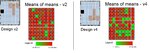
Take a look at the attachment file. The green and red dots show the mean frequency (over some rounds and some fpgas) of 80 ROs.
I'm pretty sure that the lower frequencies arise from a lower power supply and the higher frequencies from a higher one. This seems to be depending on the routing for each design.
Is there a way to see how single LEs are connected to the power supply in the chip planner?
The basic question is:
How is the power supply realised for the LABs and LEs on Cyclone IV?
Depending on where I put the control logic (without moving a single cell of the ROs), the frequencies of each RO changed.
Take a look at the attachment file. The green and red dots show the mean frequency (over some rounds and some fpgas) of 80 ROs.
I'm pretty sure that the lower frequencies arise from a lower power supply and the higher frequencies from a higher one. This seems to be depending on the routing for each design.
Is there a way to see how single LEs are connected to the power supply in the chip planner?
The basic question is:
How is the power supply realised for the LABs and LEs on Cyclone IV?