Continue to Site

Welcome to EDAboard.com

Welcome to our site! EDAboard.com is an international Electronics Discussion Forum focused on EDA software, circuits, schematics, books, theory, papers, asic, pld, 8051, DSP, Network, RF, Analog Design, PCB, Service Manuals... and a whole lot more! To participate you need to register. Registration is free. Click here to register now.

Power supply independent bias circuit

Status
Not open for further replies.

viperpaki007

Full Member level 5
Joined
Jul 2, 2008
Messages
270
Helped
11
Reputation
22
Reaction score
8
Trophy points
1,298
Location
Finland
Activity points
3,395
Hi,

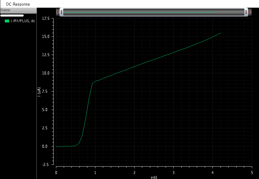
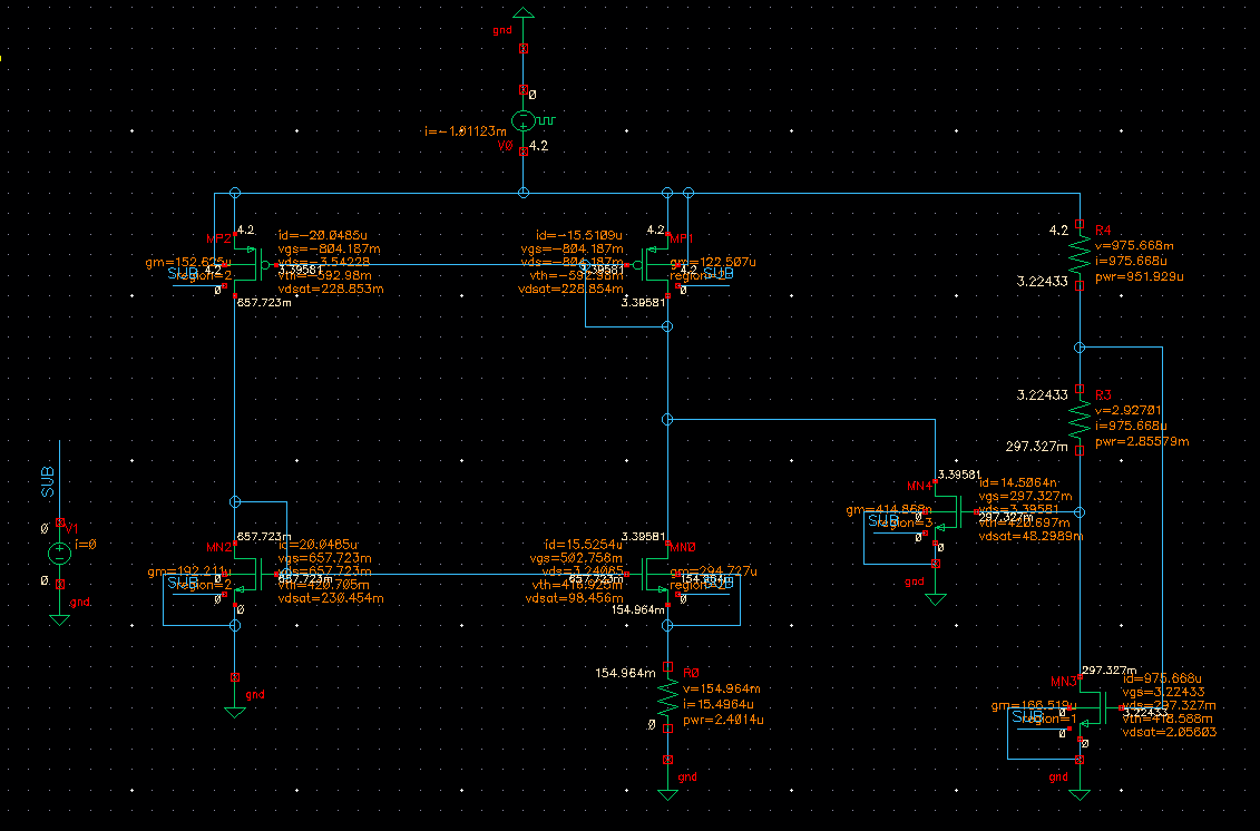
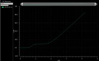
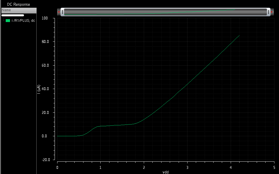
I am making a supply independent bias circuit as shown in Razavi CMOS integrated circuit book (Figure 11.5). I simulated the circuit but it does not seem to work properly. See output current vs vdd supply curve attached with this email. Can some body help? Circuit has following W and L values:

MN0 W= 28u L=1.4u
MN2 W= 7u L=1.4u
MN3 W= 7u L=1.4u
MP1 W= 14u L=1.4u
MP2 W= 14u L=1.4u


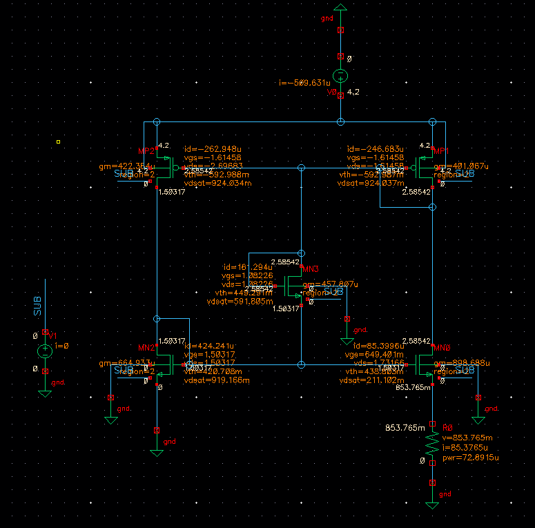
Moreover, i really can't understand how the start up circuit consisting of MN3 works. Can somebody explain this as well.

regards
 

The V/I characteristic suggests that the voltage conditions for the start-up circuit are met between about 1 and 1.8 V Vdd. You may want to refer to the Figure 11.37 start-up circuit instead.
 
Thanks FvM. However, can you explain how the start up circuit really works.. I really can't get that. Also the start up circuit in figure 11.37
 

Hi Fvm,

I designed the power supply independent bias circuit as mentioned in Figure 11.37. Simulation results are shown in figures attached. What i have understood that the startup circuit MOS transistor MN4, gate voltage (Va) should be higher than Vth in the beginning and lower than Vth after some time. This is to make sure that MN4 turns off after some time. Transient simulations show that MN4 gate voltage works in such way (Vth=420mV). However, when i see the output current vs supply voltage then i can still see variations of output current due to supply voltage change (see figure attached). Therefore, circuit is not working as it is supposed to work. Any suggestions?


Hi mate,

In calculations currents through branches are approximated to be the same. As you can see in your case, there is 30% difference between them. Therefore, circuit is not operating ok. First, try to increase widths and especially lengths of all transistors. These bottom one have to be huge (I am using L=10u for bottom ones). If this does not help, then you can cascode current mirror on top to obtain same current through both branches. However, you will always have some small dependence on power supply, it is a trade-off between area and accuracy. This paper is very helpful:
https://ieeexplore.ieee.org/xpl/art...ueryText=Fast+Startup+CMOS+Current+References
 
Thanks jkatic, Thanks for the suggestions. I increased the lengths and now the circuit is working much better than before. variations of output current have reduced.
 

Status
Not open for further replies.

Part and Inventory Search

Welcome to EDABoard.com

Sponsor

Back
Top