Continue to Site

Welcome to EDAboard.com

Welcome to our site! EDAboard.com is an international Electronics Discussion Forum focused on EDA software, circuits, schematics, books, theory, papers, asic, pld, 8051, DSP, Network, RF, Analog Design, PCB, Service Manuals... and a whole lot more! To participate you need to register. Registration is free. Click here to register now.

power and ground connection between multiple components

Status
Not open for further replies.

yefj

Advanced Member level 4
Joined
Sep 12, 2019
Messages
1,189
Helped
1
Reputation
2
Reaction score
3
Trophy points
38
Activity points
7,172
Hello, i have 4 types of components on my board shown bellow

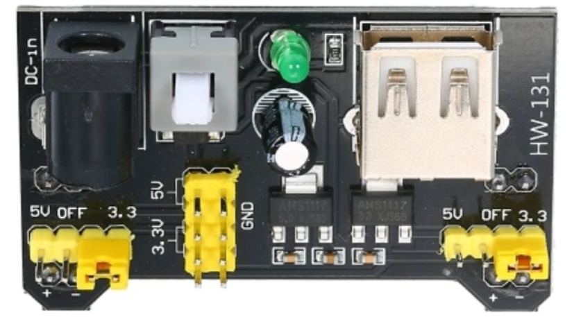
power supply :
Mini Power Supply Module HW-131 Breadboard Power Module 3.3V/5V Power Supply Module for Arduino MB102 Breadboard

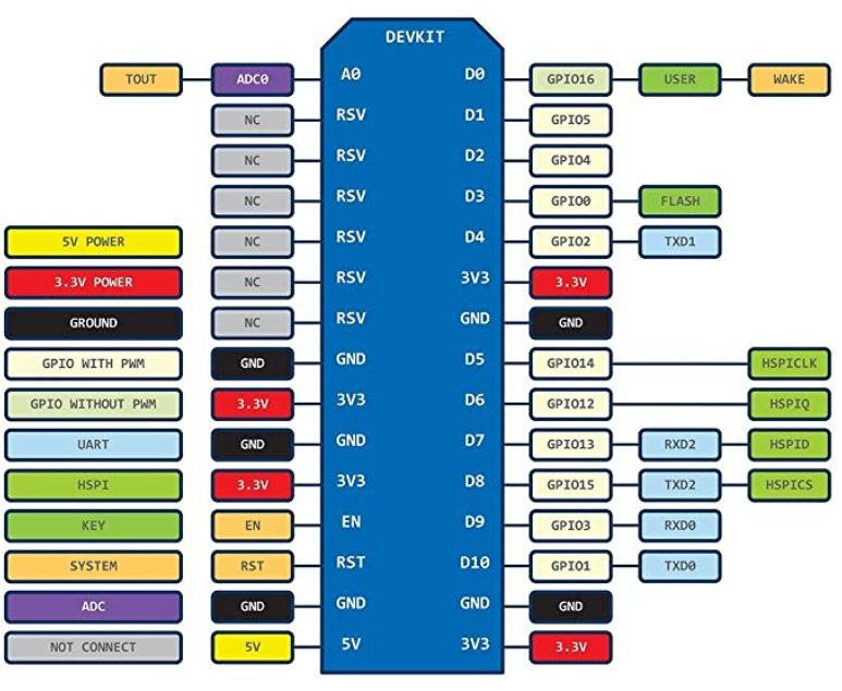
The first one is the Nodemcu ,i have two of those with the pinout map shown bellow.

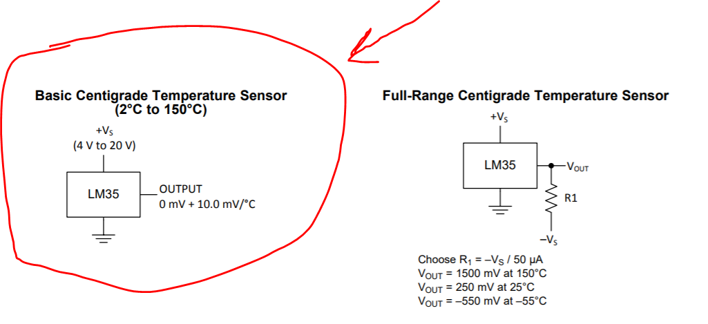
The second is : LM35DZ TO-92 LM35 Precision Centigrade Temperature Sensor with the datasheet shown bellow
.
from the data sheet we can see that it needs at least 4 volts.


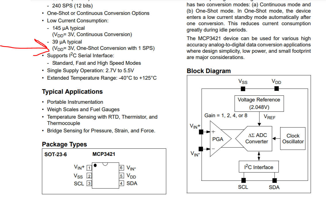
The third component is : MCP3421 I2C SOT23-6 Delta-Sigma ADC with the data sheet shown bellow.


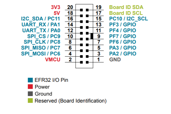
The 4th type is EFR32fg14 expantion header : from page 9 of the data sheet shown bellow.


On the bottom side of the board i have USB connection which produces 3.3V and 5V simultaniosly.
And i have the Brain wires which is the EFR32 expansion header which controlles the ADC and it has 3.3V and 5V.
So i have 2 different independant power sources. and i have a senson which needs 5 V the ADC which need 3.3 and NODE MCU which is powered by micro USB .
I dont want to power the NODEMCU devices by microusb,i want to use the general power sources(either from efr32 expantion header or the bottom power supply on the board)

another problem is the GND of all of them.

How do you recommend connecting the SUPPLY and GND of all the devices on the board bellow?
Thanks.
1608379963193.png


1608379837828.png


1608379198010.png

1608382616253.png

1608378784807.png


boards.jpeg
 
Last edited:

Hi,

good thing is that you have recognized the GND and supply problem.
The problem is the GND bounces with the according GND current...and depends on the GND line impedance.

So the problem can be avoided by an almost zero GND impedance. A breadboard is rather unsuitable with this.
Usually one uses a PCB with solid GND plane.
The problem also can be reduced by a good GND wiring concept. No GND loops. or star point connection.

The most critical will be the analog temperature sensor. It ´s output is with respect to it´s GND voltage. If this GND voltage differes from the "measurement_GND" then you will read wrong temperature values.

BTW: do you use the ADC to read the LM35 temperature? If so, i think it´s a rather unsuitable combination. On one side there is the analog GND voltage problem which may cause several millivolts of deviation and on the other side a 18 bit ADC with a resolution in the microvolts range. The least significant 7 bits (more or less) may be of no use.
There are cheap I2C temperature sensors, which will give way better performance... and many of them work with 3.3V.
There even are I2C ADCs with built in temperature sensor, so two things in one.

The ADC seems to have differential input. This may help to reduce GND bounce errors.

A big problem surely is the pulsed current consumption of the NODEMCUs.
No big problem for a digital system, but surely for an analog signaling system.

Klaus
 
  • Like
Reactions: yefj

    yefj

    Points: 2
    Helpful Answer Positive Rating
Be aware of capacitor technology effectiveness in bypass applications -

1608383113842.png


Some ap notes on PCB layout. They also apply, somewhat, to your proto work -


Regards, Dana.
 
  • Like
Reactions: yefj

    yefj

    Points: 2
    Helpful Answer Positive Rating
Hello Klauss,I have replaced the sensor with a voltage divider,and i am inputing my ADC 2.5V single ended.
I have connected the devices to common ground as shown in the updated photo bellow.
i am using EFR32FG14 board expansion header to communicate The ADC at 100Khz
and communicating the EFR32FG14 board expansion header with nodemcu by SPI at 1Mhz.
I plan to connect the GND of the EFR32fg14 expantion header to the GND of the breadboard.
How to make sure that the communication speeds are ok communication wise?
Thanks.


board_updated.jpeg

--- Updated ---

Hello Dana,what manual should i use to optimise my breadboard GND connections?
Thanks.

Be aware of capacitor technology effectiveness in bypass applications -

View attachment 166483

Some ap notes on PCB layout. They also apply, somewhat, to your proto work -


Regards, Dana.
 
Last edited:

Hi,
I have replaced the sensor with a voltage divider,and i am inputing my ADC 2.5V single ended.
Why?
I expect a really noise free digital output signal. Noise free? From an ADC? Usually impossible.
But in your case I expect it, because I expect the digital output to be saturated..
What do you think will be the digital output with (+2.5V -0.0V) = +2.5V input while the decodable input voltage range is just +/-2.048V?
I expect 0x01 1111 1111 1111 1111.
--> connect a useful input voltage.

Btw: 5V from a USB-style power supply, with pulsed load current and no good bulk capacitor, no fast decoupling capacitor, no low pass filter at voltage divider ... will not give clean 2.5V to the ADC. I won´t be surprised if 11 of the 18 bits just show noise. I don´t expect a more meaningful result than from an 8 bit ADC.


How to make sure that the communication speeds are ok communication wise?
...by reading datasheets. At least this is how I´d do it.

Klaus
 

The links I posted are general guidance to grounding. No specific manual
per se.

Regards, Dana.
 

Hello Klauss, From ADC theory my Full_scale is 3.3V so LSB=3.3/2^18=0.0000125885009765625
so if i want to sample 1.5V for example then the digital representation will be
1.5/LSB=119156.3636363636363636363 which is in binary 011101000101110100 if we cutoff the numbers after decimal point.

I know that there is quanization noise and KTC NOISE and general white noise,I am ok with recieving 1.49 results.
1.49/LSB=118361.9878787878787878 assume we use only decimal 118361 its 011100111001011001 in binary ,which is 1.489.

You said a very good thing bellow especially " with pulsed load current and no good bulk capacitor"
If i understand you correctly you say i should filter high frequency tones from the VDD source.
So we need to use an inductor ,not a capacitor.(RF choke)

What value do you recommend?
Also putting LPF after the voltage divider its a serios impedance game.
I dont know how to monitor if its getting better or worse.
How can i monitor these things? i have a spectrum analizer but i am not sure how to use it to see visually if the added components you reccomended get the signal better.

Thanks.


"Btw: 5V from a USB-style power supply, with pulsed load current and no good bulk capacitor, no fast decoupling capacitor, no low pass filter at voltage divider ... will not give clean 2.5V to the ADC. I won´t be surprised if 11 of the 18 bits just show noise. I don´t expect a more meaningful result than from an 8 bit ADC. "

1608397870602.png
 
Last edited:

Hi,
From ADC theory my Full_scale is 3.3V so LSB=3.3/2^18=0.0000125885009765625
No. It depends on the used ADC. Thus there is a datasheet.
For your ADC the datsheet says: VRef is 2.048V nominally and it has a decodable input voltage range of +/-VRef which is +/-2.048V.
(assuming G=1)

so the total input range is 2x 2.048V = 4.096V which corresponds to 2^18 as digtal output value.
One LSB represents 4.096V / 2^18 = 15.625uV
btw: clearly stated in the datasheet Table 4-1:

***

Quantisation noise and all other ADC noise and unlinearities will be ignorable compread to the VCC noise and fluctuations.
ADC is a precision part, but a power supply is something unprecise.
Compare the "ADC" with the steel ball of a bearing. Clean, shiny, almost perfectly round...wone ball has almost exactly the same size as the other.
Compare the "power supply" with random stones. Dirty, different colors, different sizes, different form, different, some are strong, some are weak.
Where the ball bearings are good for a bearings --- the stones a good to build roads. (no one will do it the other way round)

***

You compare "noise" with a fixed deviation from 1.50V to 1.49V.
But this we call accuracy error.

"Noise" never is fixed. It will move all the time.
Thus the noise of your ADC is given with 1.5uV RMS .. but don´t forget the "RMS".
With a rule of thumb you may expect a 1.5uV x 6 = 9uVpp noise. (which for me seems unrealistic on a ADC with 15uV resolution).
This is ADC noise. So you may expect it to be around 1 LSB.

But the 5V supply easily jumps by 100mV in your case. divided with your voltage divider it still is 50mV.
50mV means 3200 LSB. Which means more than 11 bits of noise. Without filter.
Now - good thing for noise - the ADC has an integrated low pass filter. It´s cutoff frequency is around 2Hz. This will reduce ouput noise significantly.
Still I expect more than 256 LSB noise. (depends on the NODEMCU current behaviour when WiFI and bluetooth is active)..this is just an asumption - maybe I´m mistaken.
So from the 18 bit there maybe are 11 true informative bit remaining.

***
A capacitor will filter. But you may additionally add an inductor.
It´s not only high frequency, even the low frequency pulsing caused by the WiFi and bluetooth operation.
I´m not speaking of the GHz frequencies. I´m speaking of the modulation frequency.
Use a scope and see what happens.
Or look at the ADC values when you set to 12 bit mode and a data rate of 240Hz.

***
What you need to take car of:
* GND bouncing or GND_Reference bouncing. When the ADC "sees" a different GND voltage than the sensor it will lead to errors.
* analog value filtering: use a suitable C connected to ADC_GND and ADC_input
* Don´t use VCC (which you currently do with the voltage divider) as reference at all. Use a separate regulator, a zener, a true reference... when you need high quality measurement values.

And not to forget: Read the ADC datasheet thoroughly. MICROCHIP also provides additional documents: Application Notes and User Guides.
They tell you how to use this ADC. And they are for free .. made for circuit designers...

Klaus
 

Status
Not open for further replies.

Part and Inventory Search

Welcome to EDABoard.com

Sponsor

Back
Top