Continue to Site

Welcome to EDAboard.com

Welcome to our site! EDAboard.com is an international Electronics Discussion Forum focused on EDA software, circuits, schematics, books, theory, papers, asic, pld, 8051, DSP, Network, RF, Analog Design, PCB, Service Manuals... and a whole lot more! To participate you need to register. Registration is free. Click here to register now.

Power Amplifier Design - Revision

Status
Not open for further replies.

julian403

Full Member level 5
Joined
Feb 28, 2014
Messages
254
Helped
1
Reputation
2
Reaction score
1
Trophy points
18
Location
Argentina
Activity points
2,105
Hi I still doing the power amplifier. I made the next power ampliffier step

circuito.png

Icmax= 4.3 [A] and the HFE is about 100 so I need a Ibmax=0.03 [A]. But I do not know how make the driver step.

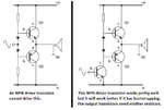
I thought use a TIP41 as commun emitter

circuito2.png

Where the output of this step is on colector. So, the output impedance that it will see is:

10 [KΩ] // (8.1 [Ω])(HFE+1)

Where the last HFE is the 2SA5200's HFE. But when I try it on the simulator it does not work. What do you thinks? What I must use as driver step? (to drive a current of 0.03[A] on the 2SA... transitor's base?
 

You must inject the signal between both diodes so with a minimum voltage the B-E junctions will polarise. Your circuit is wrong.

About the current, its limit is defined by the resistor connected to the power rail (+V/GND). With a basic ohm law formula you can calculate the resistor value to let that current.
 
About the current, its limit is defined by the resistor connected to the power rail (+V/GND). With a basic ohm law formula you can calculate the resistor value to let that current.
What circuit do you means? the drivers?

- - - Updated - - -

and the point bettwen the diodes is ground? I think it is.
 

The circuit will only work if you can provide bias current for BOTH transistors from the driver stage. Remember to keep the transistors conducting you need to keep the BE junction forward biased so consider that in respect to the emitter voltages as the output point voltage changes.

The center point between the diodes is NOT ground. If you ground it you will limit the input voltage range (which is more than the output voltage range!) to about +/- 0.7V.

To make it work properly you should thermally bond the diodes to the transistors to give it some thermal stability and use the voltage at the output point to stabilize the bias of the driver stage. To be honest, a better bias arrangement than two diodes would be very advisable.

Brian.
 
Why do you think I get this output signal?, with just 10[V] input signal peak

ccc.png
 

Something is wrong with your simulator setup.
 

Attachments

  • power.png
    power.png
    27.6 KB · Views: 77
what software do you use E-design? I need 2SA5200 and 2SA1943 transistor and ISIS proteus has not
 

I do not think anybody produces an amplifier where the driver's collector is connected between the diodes and one resistor pulls up the base of the NPN and another resistor pulls down the base of the PNP.
Usually the driver transistor is NPN and its collector is connected to the base of the PNP output transistor and a pull up resistor (or a current source) connects to the base of the NPN output transistor.
 
It work now, but for a input signal of 10[mV] there is a little mor of 200[mV] output. for an input signal of 40 [mV] it saturates. And I need a input signal of 1.2[V]

img0.png

img1.png

it more difficult that I thought

PD: I modified the TIP31 and TIP32 to withstand voltage 140V , as the 2SA5200 and 2SA1943
 
Last edited:

R11 and R12 bias the output transistors with a current that is way too low!.
If the maximum peak output into the 8 ohm speaker is 60V then the output power is 225W RMS. Each transistor will overheat dissipating about 90W of heat each.
The peak current of each output transistor is 60A/8 ohms= 7.5A. With the 70V power supply voltages then the minimum base current when the output is 60-V peak is about 9V. So the base current at the peak output current is only 9V/10k ohms= 0.9mA but some of this very small current goes into the diodes.
Then the transistors must have a minimum hFE of more than 7.5A/0.9mA= 8333 but their hFE is MUCH less.

You need an NPN driver transistor to pull down the base of the PNP output transistor with a maximum current of maybe 750mA and you need a fairly low value pullup resistor to pull up the base of the NPN output transistor with a maximum current of maybe 750mA. Didn't I post this circuit already?

I think with such a high maximum output current you need a pair of driver transistors to drive the output transistors.
 

Attachments

  • amplifier.png
    amplifier.png
    30.8 KB · Views: 75
You can connect transistors in parallel (with their own emitter stabilizer resistor) to increase the maximum total current. How much power do you want it to supply? The common collector class AB circuit has no voltage gain so the input voltage must be amplified to get the highest power
 
I want a power load of 150 W. I now it's to much source for that but the circuit was done wrong from the beginning. I'am going to do it and post it here and I'll see what comes to me to ask you
 

Do you know the simple formulas to determine the voltage and current swing in an 8 ohm load with 150W RMS?
The voltage is the square root of (150W x 8 ohms)= 34.64V RMS. The peak voltage is 34.64V x 1.414= 49.0V and the p-p voltage is 49V x 2= 98.0V.
Then the current is 150W/34.64V= 4.33A RMS which is 6.12A peak.

You need output transistors that have a voltage rating of more than 98V and a current rating more than 6.12A. You cannot buy transistors with a "typical" hFE so use the minimum hFE listed on the datasheet for 6A which might be only 15. Then the peak base current is 6.12A/15= 408mA which indicates that you need driver transistors.
 

I want a power load of 150 W. I now it's to much source for that but the circuit was done wrong from the beginning. I'am going to do it and post it here and I'll see what comes to me to ask you

This circuit that I have taken based on ON Semiconductor's NJL0281D (NPN) and NJL0302D (PNP) gives 200W @ 4Ohm Full Bridged configuration.THD=0.025% at Full Power, BW=10Hz-22kHz and ti may be of course more improved.Just an idea..

Audio_PA.png
 

This circuit that I have taken .......
1) Why are there very distracting red dots all over the wiring?
2) Why are the power supplies not connected to the circuit?
3) Why are R? and R? not connected to anything?
4) Why are there dozens of diodes?

The diodes built into the package of each output transistor are not parallel with the collector-emitter, instead they are separate but thermally tracking bias diodes for biasing the bases of the driver transistors.

I found a similar amplifier schematic (not bridged) as an applications note from ON Semi that does not have red dots all over the place (caused by your schematic software?)
 

Attachments

  • amplifier from ON Semi.png
    amplifier from ON Semi.png
    52.2 KB · Views: 79

1) Why are there very distracting red dots all over the wiring?2) Why are the power supplies not connected to the circuit?3) Why are R? and R? not connected to anything?4) Why are there dozens of diodes?The diodes built into the package of each output transistor are not parallel with the collector-emitter, instead they are separate but thermally tracking bias diodes for biasing the bases of the driver transistors.I found a similar amplifier schematic (not bridged) as an applications note from ON Semi that does not have red dots all over the place (caused by your schematic software?)
Don't worry, the red dash lines are conencted, it's just a Cadence warning.Power supplies are also connected well at netlist based.The symbols represent only transistor+diode modules only.Diodes are in transistors package and they act as accelerator against temperature rising.Scematic of App. Note of ON Semiconductor is almost same except some tweaks to improve frequency response and the stability..
 
Last edited:

Your Cadence schematic is Very Confusing with blue and green lines all over the place. I removed the green lines and some of the red dots and it looks much better.
 

Attachments

  • Cadence amplifier schematic.png
    Cadence amplifier schematic.png
    20.9 KB · Views: 70

Your Cadence schematic is Very Confusing with blue and green lines all over the place. I removed the green lines and some of the red dots and it looks much better.

But the others will think the diodes are seperated from the transistor but they are integrated in a singla package..
 
Status
Not open for further replies.

Similar threads

Part and Inventory Search

Welcome to EDABoard.com

Sponsor

Back
Top