Continue to Site

Welcome to EDAboard.com

Welcome to our site! EDAboard.com is an international Electronics Discussion Forum focused on EDA software, circuits, schematics, books, theory, papers, asic, pld, 8051, DSP, Network, RF, Analog Design, PCB, Service Manuals... and a whole lot more! To participate you need to register. Registration is free. Click here to register now.

Positive and negative planes

Status
Not open for further replies.

raj_pcbtech

Member level 3
Joined
Aug 9, 2007
Messages
61
Helped
1
Reputation
2
Reaction score
0
Trophy points
1,286
Location
India
Activity points
1,617
Hello All

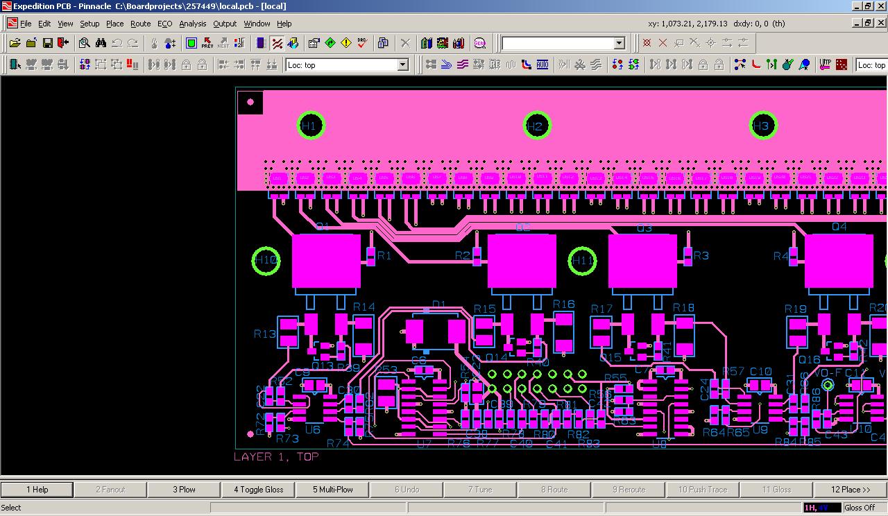
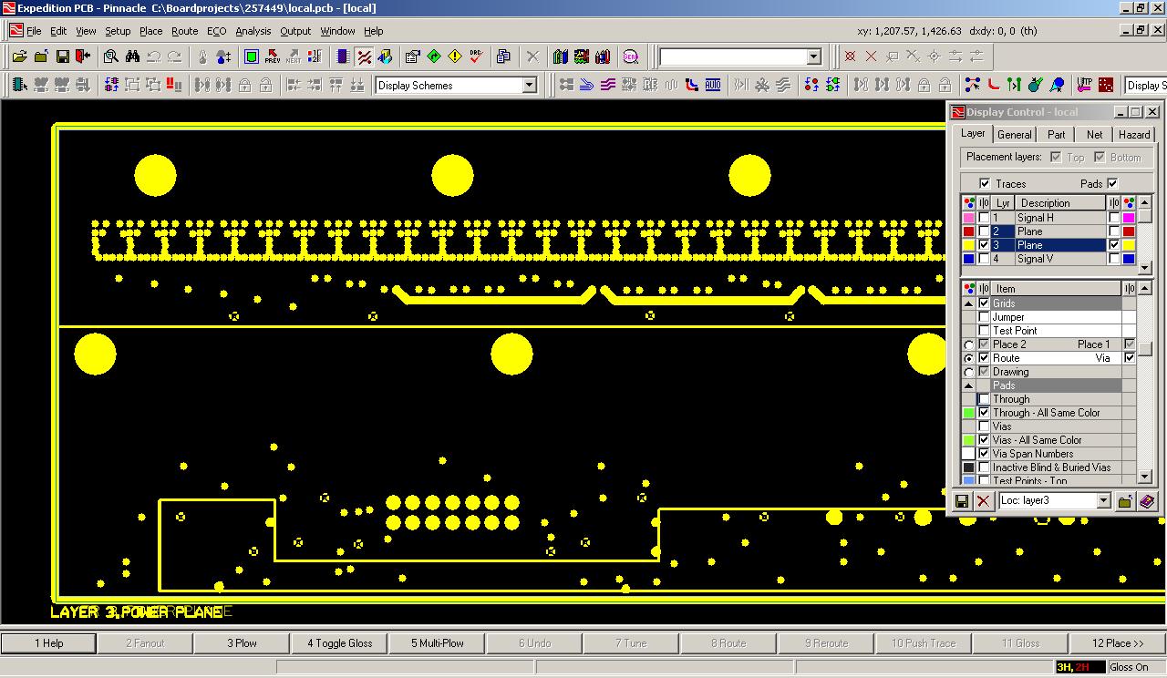
Can anyone please explain me about the difference and merits, demerits between positive and negative planes? Thanks in advance.

Rajkumar
 

Positive planes - one has to fill the copper area with vectors (traces) or in some packages, areas. When it converted to Gerber files, most of the packages will convert filled areas into smaller vectors and it will result in increased Gerber file size.
If negative layers are used, this can be avoided and also it is easier to draw the split planes in negative as we need to draw the vectors comprising the devided area between two planes.
 

I understand it. But would you please upload some snap shots of both positive and negative planes?
Any help would be greatly appreciated.

Rajkumar R
 

First file is a positive plane (top layer)
Second file is a Negative plane (Internal layer2 of a 4 layer board)


On the positive planes, the area surronding the traces and pads are etched away from the copper layer.

On the Negative plane, what shows are pads and thermal reliefs are etched out of the copper, so the black area on this picture is actually solid copper.

I've also done Positive layers on internal layers where I need to put traces and copper areas in the layout - that would look the same as the Top layer pic.
And, traces can also be embedded in Negative layers, where the net/trace would have an enclosed outline around it to create a mote of conductivity.
 

If we use negative planes,our file size wll be less..so it is easy to handle multilayer layer boards with the use of negative planes.

But lots of problem comes when u verify/Check the design.it requires lots of attention.

if we have better system configuartion then we can easily handle multilayer boards with positive planes.
I prefer to use positive planes
 

Status
Not open for further replies.

Part and Inventory Search

Welcome to EDABoard.com

Sponsor

Back
Top