Welcome to our site! EDAboard.com is an international Electronics Discussion Forum focused on EDA software, circuits, schematics, books, theory, papers, asic, pld, 8051, DSP, Network, RF, Analog Design, PCB, Service Manuals... and a whole lot more! To participate you need to register. Registration is free. Click here to register now.
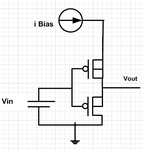
Hi, I have come across an amplifier which I don't understand how it works. It is using 2 pmos transistors. It does not look like any of the source followers I have seen. Can someone explain the attached cicuit to me? Thank you.
Hi Baseball 07 !
Is your Vin , a DC signal ?? let me confess a thing ! it is like a digital gate ! i have seen circuits such as that , in digital gate design approaches .
Before trying to help you , i think one of your mosfets is N type and the other one is P type . am i right ?
If yes , it's analysis is too easy . which section is unclear fro you ?
Best Wishes
Goldsmith
Thank you very much for your reply. Yes it is a DC signal, and it is 2 pmos. The whole thing is unclear to me, can you please give me a brief analysis on it? Thanks for the help.
This is not a follower then you need AC signal as input and have to get that as op here the op will be the Vdd voltage alone and not any followed signal as there is no signal to follow or amplify
Hi, thank you. I am not sure I understand what yuo ae saying. I don't really know what it is called, whatever the name for it is, I don't understand its operation.
It is actually used as a level shifter. However I don't understand the S/D connected PMOS aspect of it. Why not just feed the lower PMOS current directly?
Ok I understand now. Essentially, the current though the pmos channel produces the source voltage at the bottom pmos. Could an nmos be used instead if it just providing resistance? What is the name of the MOSFET configuration when the S/D are shorted like that?
Source to drain shorted PMOS will work as capacitance only. As far as the architecture is concerned , it is used for level shifting at output, shorted PMOS works as Cgs capacitance, may be exploited for miller capacitance.
This site uses cookies to help personalise content, tailor your experience and to keep you logged in if you register.
By continuing to use this site, you are consenting to our use of cookies.