Matmat45750
Newbie
Hello everyone,
I am designing my first PLL.
The input clock will be around 32.786 kHz and the VCO's free running frequency is at 32.786 kHz. I am currently trying to estimate the VCO's and input clock's phase noise to set the optimized bandwidth and then get the minimum output jitter.
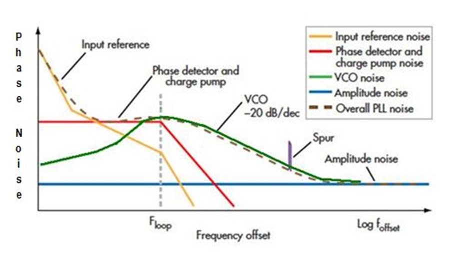
I have studied many PLL's phase noise profile and most of them look like this one:

I have understood that the frequency offset is (in my case) Foffset = Real_frequency - 32.786 kHz (carrier_frequency)
Then taking a look to this plot I understand that F_loop (PLL Bandwidth) is higher than the carrier frequency, but I have also read than 1/20*carrier_frequency < F_loop < 1/10*carrier_frequency.
So I don't understand anymore.
Furthermore, why don't we interest to frequencies between 0 and F_carrier ? Do we consider that the phase noise profile is symmetric ? It would be weird because for each PLL's component the output phase noise is Sout = Sin*H^2
with : - Sout: the phase noise at the PLL's output due to the component (PFD or VCO or Input clock ...)
- Sin: The phase noise due to the component (PFD or VCO or Input clock ...)
- H: The transfer function from the component's input to the PLL's output
And H is either a low (Input clock) or a high (VCO) pass filter, then it is not symmetric.
Thank you very much to all of you.
I am designing my first PLL.
The input clock will be around 32.786 kHz and the VCO's free running frequency is at 32.786 kHz. I am currently trying to estimate the VCO's and input clock's phase noise to set the optimized bandwidth and then get the minimum output jitter.
I have studied many PLL's phase noise profile and most of them look like this one:
I have understood that the frequency offset is (in my case) Foffset = Real_frequency - 32.786 kHz (carrier_frequency)
Then taking a look to this plot I understand that F_loop (PLL Bandwidth) is higher than the carrier frequency, but I have also read than 1/20*carrier_frequency < F_loop < 1/10*carrier_frequency.
So I don't understand anymore.
Furthermore, why don't we interest to frequencies between 0 and F_carrier ? Do we consider that the phase noise profile is symmetric ? It would be weird because for each PLL's component the output phase noise is Sout = Sin*H^2
with : - Sout: the phase noise at the PLL's output due to the component (PFD or VCO or Input clock ...)
- Sin: The phase noise due to the component (PFD or VCO or Input clock ...)
- H: The transfer function from the component's input to the PLL's output
And H is either a low (Input clock) or a high (VCO) pass filter, then it is not symmetric.
Thank you very much to all of you.