Welcome to our site! EDAboard.com is an international Electronics Discussion Forum focused on EDA software, circuits, schematics, books, theory, papers, asic, pld, 8051, DSP, Network, RF, Analog Design, PCB, Service Manuals... and a whole lot more! To participate you need to register. Registration is free. Click here to register now.
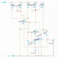
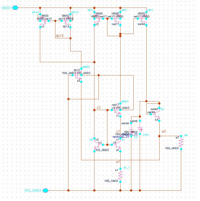
could anyone please explain to me the operation of the circuit below? i know this is a bandgap but i confuse for the part Q3, R and why there is a cap.
Q1=8Q2
Thanks a lot first.
another question is, what is the difference between model "nanch3" with "nch3" for TSMC .18u process?
Q3 connected as a diode to provide a CTAT voltage. PTAT current flows from R3 to provide a PTAT voltage. Left side circuit including MNN2 seems to be a startup one. caps here is to stabilize the reference voltage!
nanch3 is a n-channel mosfet which acts as a native transistor. No threshold adjustment mask will be added in the fabrication process!
hi Allan_guo, could you explain further how MNN1 used for startup? and more detail explanation on MNN2 to reduce system error?
Initially i thought MNN2 is as startup circuit for this bandgap.
hi jianjing526,
nanch3 is native transistor and no threshold adjustment mask added, does it means that there is no extra layer needed for this MOS? Am i correct?
This site uses cookies to help personalise content, tailor your experience and to keep you logged in if you register.
By continuing to use this site, you are consenting to our use of cookies.