Welcome to our site! EDAboard.com is an international Electronics Discussion Forum focused on EDA software, circuits, schematics, books, theory, papers, asic, pld, 8051, DSP, Network, RF, Analog Design, PCB, Service Manuals... and a whole lot more! To participate you need to register. Registration is free. Click here to register now.
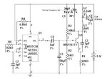
Actually should read "frequency setting trimmer ". It is a variable capacitor and is used to fine tune the transmit frequency to match the cell phone freq.
If I am not mistaken, then the output frequency (from the 555 pin3) calculation comes out to be 8.4MHz with the present set of resistors (6.8K+82K) and capacitor (1pF). I don't think that a 555 even with CMOS version can handle such a high frequency>>>
Yes, but what's the conclusion? Obviously, your formula doesn't apply. Did anybody claim, it should? I assume, it's still operating, but at a lower frequency, may be 1 MHz. Considering the obscure precision values of some parts, some values may be simply mistyped.
Generally, it looks like a kind of rather uneffective cell phone jammer, a transmitter not taking care of any serious RF regulations anyway. A toy for bored school boys.
This schematic seems like a failed attempt to design a jammer... The Hartley oscillator is wired for approximately 513MHz and the 555 timer output (obviously a wrong design... the chip cannot handle more than 1MHz... and it is not true that it will create a 1MHz even if it is designed for a much higher frequency.. 8.4MHz)...
I think he basic aim was to mix the two frequencies... (f1+f2 or f1+2f2 ...) Still it is really hard to reach the cell band... The harmonics will not be that strong!
This site uses cookies to help personalise content, tailor your experience and to keep you logged in if you register.
By continuing to use this site, you are consenting to our use of cookies.