Continue to Site

Welcome to EDAboard.com

Welcome to our site! EDAboard.com is an international Electronics Discussion Forum focused on EDA software, circuits, schematics, books, theory, papers, asic, pld, 8051, DSP, Network, RF, Analog Design, PCB, Service Manuals... and a whole lot more! To participate you need to register. Registration is free. Click here to register now.

Placement of bypass capacitor

Status
Not open for further replies.

swen_s

Member level 1
Joined
Nov 29, 2012
Messages
40
Helped
1
Reputation
2
Reaction score
1
Trophy points
1,288
Activity points
1,598
How is the best way to connect bypass capacitors to an IC?

The one (green) I made. Would it be better than a and b?

bypass.png
 

It depends. If you are most concerned with providing a very low impedance on the chip's Vcc rail, then your approach is fine. But it you concerned with that chip injecting interference into the power planes, then I would go with B.

For your version, there's really no reason to have two vias on one VCC trace. Or if you do have multiple vias, you shouldn't put them in between the cap and the IC.
 
It would be better to go with b.
 

Surely B is the correct way!! You are placing cap to bypass noise and power sources generates noise...
 

your method seems to be a composite of a and b, and probably better than either.
 

It depends on the frequencies involved. My preference is not to have vias between the decoupling capacitor and the IC - they add inductance; not much, but at 500MHz or more you will notice it. So, I would put the vias to the left of the decoupling capacitor and directly decouple the IC with the PCB tracks. Some IC pinouts make that impractical so you have to use vias somewhere between the decoupler and the device.

Keith.

good point. but what about the inductance of the tracks ? would that be less than that of a via ? Your post implies it is so - where can we get info about this comparison ? i know i can google, but some instant wisdom always helps ;-)
 

There is software around to calculate the characteristics of vias and tracks (Saturn PCB is one). You are right about the inductance of a track - that needs considering - and I would make the tracks wider than shown. I have probed vias on high speed layouts on both sides of the PCB and seen the effect of the via inductance on the decoupling. These were analogue circuits - broadband amplifiers which amplify analogue pulses. The via inductance was sufficient to show resonance with the decoupling capacitance which caused a disturbance on the flat frequency response. Unfortunately I don't have the spectrum analyser traces from the work - made the observations, made some changes and moved on.

Keith.
 

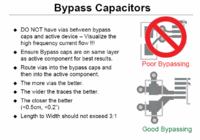
some words of wisdom (i suppose) from a TI paper on high speed design

* DO NOT have vias between bypass caps and active device – Visualize the high frequency current flow !!!
* Ensure Bypass caps are on same layer as active component for best results.
* Route vias into the bypass caps and then into the active component.
* The more vias the better.
* The wider the traces the better.
* The closer the better (<0.5cm, <0.2”)
* Length to Width should not exceed 3:1

there's lots more which looked good ... https://www.ti.com/lit/ml/slyp173/slyp173.pdf
 

A is the correct way it gives the lowest possible inductance, which is the controlling factor in cap placement and achieving the best decoupling.
There are numerous data sheets and application notes on bypassing, try the AVX site and ALL the chip manufacturers sites.
The shortest route is doublesided placement with the caps as near the pins as possble.
Also use the smallest package size available for a chosen value of capacitance, and two vias per pin.
Once you get above 50MHz it is the interplane capacitance that is the main current source during switching.
Lost my list of links but heres one good one:
http://www.hottconsultants.com/techtips/decoupling.html
 
Last edited:

A is the correct way it gives the lowest possible inductance, which is the controlling factor in cap placement and achieving the best decoupling.

Surely that increases inductance by adding vias between the decoupling capacitor and the device? It also contradicts the TI document linked to by kripacharya.

Keith
 

I have over 200 documents regarding decoupling and bypassing capacitors, a few are referenced in the attached txt file. I do mainly high speed designs these days, using this software to simulate the actual power delivery syste:
http://www.algozen.com/DS_CADSTAR_LT_PowerIntegrityAdvanced_ENG_2011_10_05.pdf
What people forget or dont realise is that the bypass capacitors are not supplying the pin directly with charge but are supplying the interplane capacitance with charge. The charge is supplied in bucket brigade fashion as follows:
On die caqpacitance.Plane capacitance.
small bypass capacitors.
Reservoir capacitors.
Power supply.
The text document has some figures for this, from an older Ti document, where 250MHz is used, but with recent software simulation advances and empirical measurments these days the figure is reckoned to be nearer 50MHz so basicly bypass capacitors are usless above 50MHz.
Also it is worth looking at actual inductance values of vias and traces, use actual round trip figures for the via to power planes, this can be a short as 0.5mm on some high speed designs as they tend to be 8+layers and more often than not 12+ to get the correct structure for multiple ground return planes for critical signals.
This subject cannot be defined by a few simple comments, I have been studying it and the changes increased rise time have brought for over 25 years. These days I have simulation software and 3D field solvers to help me simulate and tweek designs to get them right and place decoupling capacitors to get the lowest power supply impedance for a givervoltage for a given layout. You can only do this with the right software, as Eric Bogating alwyas says these days regarding highe speed design, "No myths allowed" meaning the rules of thumb we have used for many years just dont cut it with todays designs.
Also today most designs are double sided with bypass capacitors on the rear of the board as most of the high speed parts that are critical are BGA devices, though I have done designes where 0201 bypasscapacitors were placed on the same side as the BGA between the pins, a HDI design with top layer ground plane and next layer (0.05mm dielectric) main power for the device, to minimise the decoupling loop area and distance to the absolute minimum.
 

Attachments

  • Decoupling Caps #2.txt
    755 bytes · Views: 86
Last edited:
Marce,

These documents all seem to be related to high speed digital design. My design is normally high speed analogue/RF - do you have any references which specifically deal with that? The issues there are possibly different to digital design such as gain variations caused by unwanted inductance in the decoupling path - a particular problem I have seen and is improved by ensuring you avoid vias in the decoupling path if possible, and by multiple decoupling capacitors. With tuned amplifiers it is not such a problem but most of my design is broadband where gain flatness is important.

Keith
 

Hi Keith,
to be honest on numerous designs I do have to use B froim above, but as these devices tend to be relativly low speed
it isn't as critical, and on single sided placement is often the only sensible way of routing.
RF...
I will have to look through my documentation, as we do very little RF compared to high speed and when we do
he engineer resposible for the circuit generaly dictates all aspects of the layout due to RF's ssuseptability to stray
parasitics from the layout. I have a fair bit of info as it has always been one area where I would like to learn more, becauseit is the one areaof electronics that is
'black magic'.

Marc
 

Marc,

Thanks, I would appreciate anything you may come across. I tend to follow manufacturers guidelines and it seems to be successful following the rules in the TI document; in particular:


... although I don't usually have the space to use multiple vias. I have spent a lot of time trying to get ultra-flat broadband amplifiers up to around 1GHz and the decoupling seems to be very critical in achieving this. The most telling sign is that if you probe the power supplies of a chip, the decoupling capacitors and any vias/tracks associated with them with a spectrum analyser, you can see dips or peaks in the same places that the amplifier has a dip or peak. Fixing the decoupling problem usually fixes the amplifier dip/peak.

Keith.
 

Hi Keith,
didn't get much done this weekend as I was whisked away to my Grandaughters Christening, so had no internet (or computer).
The best I have found so far is the Semtech link, below. The more I look the moreoptions and vies I find on the subject of decoupling.
Looking at different layout restrictions/styles (single sided, double sided, caps end on to pins, 90 to power pins etc)
I believe there is no single method that we can employ, but use best practice for each decoupling capacitor and how it is placed.
So the best solution is one that minimises the loop area and impedance for any given capacitor. For single sided placement, there are numerous arguments for all three options
shown in the first post. I will do some more reading and look for newer app notes etc, usually new devices are a good place for this, so I'll delve into some
manufacturers sites. For me(and many others) decoupling is becoming more problematic as BGA pitches decrease, I have a board fullof 0.5mm pitch BGA's and 0402 caps!!!

https://www.semtech.com/images/datasheet/rf_design_guidelines_semtech.pdf

**broken link removed**

https://www.analog.com/static/imported-files/tutorials/MT-101.pdf

https://www.ti.com/lit/an/sloa069/sloa069.pdf
 
Marc,

Many thanks for that - I will print those off for reading at leisure. At first glance they look interesting because they cover some of the real world problems of pins not being where you would want them so you have to use vias. Interesting about mounting capacitors on their sides. For some recent work I was trying to find capacitors which didn't have the "wrap around" ends as they increase inductance.

Keith

the side mounting only helps with moving the PRF's much higher (i think). Your SRF still needs a lower inductance design to be improved.
 

the side mounting only helps with moving the PRF's much higher (i think). Your SRF still needs a lower inductance design to be improved.

My thought was that it may also reduce the inductance of the wrap around end caps which are a significant source of the stray series inductance from what I have been reading. I would have to test it though to see.

Keith
 

Status
Not open for further replies.

Part and Inventory Search

Welcome to EDABoard.com

Sponsor

Back
Top