Continue to Site

Welcome to EDAboard.com

Welcome to our site! EDAboard.com is an international Electronics Discussion Forum focused on EDA software, circuits, schematics, books, theory, papers, asic, pld, 8051, DSP, Network, RF, Analog Design, PCB, Service Manuals... and a whole lot more! To participate you need to register. Registration is free. Click here to register now.

Pin property for symbol in DxDesigner and PADS Layout

Status
Not open for further replies.

Veronika

Member level 2
Joined
Mar 30, 2012
Messages
51
Helped
0
Reputation
0
Reaction score
0
Trophy points
1,286
Activity points
1,651
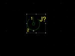
I am using DxDesigner and PADS Layout. I need to make a symbol for coaxial SMA jack, which has one signal pin and 4 GND pins.
In Layout I have 4 separate pins for GND but in Schematic I need to draw a symbol with one center (signal) pin and one outer (GND) pin.
So for GND I have one pin in Schematic but 4 pins in Layout.

How can I assign one pin in Schematic to all four pins in Layout??

Thank you in advance!
 

Hello Veronica,

You have to define this in the cell editor.

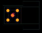
Open the cell in the cell editor and name the 4 gnd-pins the same, for example 2 or GND or whatever you prefer. The cel editor will show you the guides between the four pins. Now save the cell.
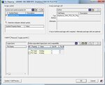
In the part editor open the pin mapping for the part, the four pins with the same name shows up as 1 pin. Map the two pins of the cell to the corresponding two pins of the symbol and save it.


symbol.jpg cell.jpg mapping.jpg


succes.
 
Last edited:

Unfortunately, when I try to name these four pins the same in PCB Decal Editor, the PADS Layout does not allow me to do this and an error appears: "Alphanumeric name is already used."
I guess I am using another version of PADS...
What should I do?
 

Hi Veronica,

u can create symbol as u want in pads schematic but u can change pcb decal in layout.
just replace current pcb decal with two pads.
 

How can I replace decal with two pads if the footprint has one pad for signal and four pads for GND?? I cannot change the number of pads for the footprint of the component I am going to use...
 

Status
Not open for further replies.

Part and Inventory Search

Welcome to EDABoard.com

Sponsor

Back
Top