Continue to Site

Welcome to EDAboard.com

Welcome to our site! EDAboard.com is an international Electronics Discussion Forum focused on EDA software, circuits, schematics, books, theory, papers, asic, pld, 8051, DSP, Network, RF, Analog Design, PCB, Service Manuals... and a whole lot more! To participate you need to register. Registration is free. Click here to register now.

[PIC] PIC16F876A strange ADC output value

Status
Not open for further replies.

ginettine

Newbie level 5
Joined
Mar 29, 2022
Messages
9
Helped
0
Reputation
0
Reaction score
0
Trophy points
1
Activity points
87
Hi, I'm Alex from Italy.
Sorry for the bad English.
I'm trying to verify what is the input voltage level on AN0 that sets the LSB to 1 (in theory 5/1024 = 4.88mV!).
On breadboard I stabilized Vdd = 5V with lm317.
I send the converted value to 10bits on portb (8 least significant bits!), And on RC0 and RC1 the two bits MSB
Problems:
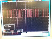
1) The Vin level that sets the LSB (RB0!) to 1 is "variable" (almost a linear ramp between about 1.8 and 5V!) Between about 6 and 8mV.
2) with an oscilloscope I see a sort of "PWM" output on RB0 with variable duty cycle, when the Vin varies between about 6 and 8mV !!!!

How is it possible?

The code in Mikroc:

Code:
unsigned int temp_res;
 
void main ()
{
  ADCON1 = 0x80; //
  PORTB = 0;
  PORTC = 0;
  TRISB = 0;
  TRISC = 0;
  TRISA.F0 = 1;


  do {
     temp_res = ADC_Read (0); //
     PORTB = temp_res; //
     PORTC = temp_res >> 8; //
   } while (1);
}

Many thanks!
Alex
 

Sorry, question is not clear. Please add following information to your question:
1. Please explain what is your expectation when Vin is between 6mV and 8mV AND what is wrong?
2. What is the partNumber of micrcontroller?
2. How are you providing Vin to the ADC?
3.
(almost a linear ramp between about 1.8 and 5V!)
--> Did the ramp occur on RB0?
--> For 4.88m<Vin<6mV, what was status of RB0?
 

First, thanks for the answer!
1) beetween 6 to 8mV, RB0 must be zero (and RB1 must be 1!).
2) Now i'm not in lab...tomorrow i'll check the part number.
3) Yes, in RB0 (every pins of portb that became 1has this "ramp"!).
4) In that range RBO increase slowly from avut 0 to some hundred of mV.

Alex
 

Hi,

An ADC has:
* offset error
* gain error
* linearity error
* noise

Thus the output is not "ideal".

You need to read the ADC specification.

Klaus
 

Hi Klaus,
Thanks for contribute!
Offset, gain, linearity errors and noise can justify the "Pwm modality" on portb?
Until now, i know that, in digital way, the output can be only
logic 0 and 1 ( not like PWM, with variabile duty cycle!)
A SAR can working in they way?
Alex
 

2) Now i'm not in lab...tomorrow i'll check the part number.
I just realized, you have given part number is PIC16F876A, I missed this in description.

3) Yes, in RB0 (every pins of portb that became 1has this "ramp"!).
Basic things I suggest to do tomorrow:

1. Add delay in code and check if any change observed in RB0 voltage pattern.
Code:
do {
temp_res = ADC_Read (0); //
PORTB = temp_res; //
PORTC = temp_res >> 8; //
delay_ms(10);
} while (1);

2. Check if LVP (Low voltage programming) is enabled and program pin are left floating (PGM Pin). This can cause unstable behaviour on GPIO.

3. In code, configure ADCON1 to select only channel 0 and try again
ADCON1 = 0x8E;


4) In that range RBO increase slowly from avut 0 to some hundred of mV.
As you mentioned ADC Step Size is 5/1024 = 4.88mV. For ideal adc, if 4.88m<Vin<488*2, RB0 must be 1. So your adc is not ideal. However I guess real problem is when LSB is 1, RB0 is ramp. Check RB0 is stable by manually setting
Code:
PORTB = 0x01;
Checking this would reveal if the issue has anything to do with adc or not.

Goodluck..
 

@ginettine,

The code you posted does not show how you have initialized the configuration words or the ADC control register ADCON0 of the PIC16F876A controller.

I do not have the MikroC compiler installed but here is as generic an example as I can create with the Microchip XC8 compiler.
C:
/*
 * File:   main.c
 * Author: dan1138
 * Target: PIC16F876A
 * Compiler: XC8 v2.35
 * IDE: MPLABX v6.00
 *
 * Created on March 29, 2022, 11:58 AM
 * 
 *                            PIC16F877A
 *                    +-----------:_:-----------+
 *         ICD_VPP -> :  1 MCLRn         PGD 28 : <> RB7 ICD_PGD
 *      ADC_IN RA0 <> :  2 AN0           PGC 27 : <> RB6 ICD_PGC
 *             RA1 <> :  3 AN1               26 : <> RB5 
 *             RA2 <> :  4 AN2               25 : <> RB4 
 *             RA3 <> :  5 AN3           PGM 24 : <> RB3 
 *             RA4 <> :  6 T0CKI             23 : <> RB2 
 *             RA5 <> :  7 AN4/SS            22 : <> RB1 ADC_bit_9
 *             GND <> :  8 VSS          INT0 21 : <> RB0 ADC_bit_8
 *      20MHz XTAL -> :  9 OSC1          VDD 20 : <- 5v0
 *      20MHz XTAL <- : 10 OSC2          VSS 19 : <- GND
 *   ADC_bit_0 RC0 <> : 11 T1OSO          RX 18 : <> RC7 ADC_bit_7
 *   ADC_bit_1 RC1 <> : 12 T1OSI          TX 17 : <> RC6 ADC_bit_6
 *   ADC_bit_2 RC2 <> : 13 CCP1          SDO 16 : <> RC5 ADC_bit_5
 *   ADC_bit_3 RC3 <> : 14 SCK/SCL   SDA/SDI 15 : <> RC4 ADC_bit_4
 *                    +-------------------------+
 *                              DIP-28
 */
/*
 * Define how this code will setup the system oscillator frequency
 */
#define _XTAL_FREQ 20000000

#pragma config FOSC = HS        // Oscillator Selection bits (HS oscillator)
#pragma config WDTE = OFF       // Watchdog Timer Enable bit (WDT disabled)
#pragma config PWRTE = OFF      // Power-up Timer Enable bit (PWRT disabled)
#pragma config BOREN = OFF      // Brown-out Reset Enable bit (BOR disabled)
#pragma config LVP = OFF        // Low-Voltage (Single-Supply) In-Circuit Serial Programming Enable bit (RB3 is digital I/O, HV on MCLR must be used for programming)
#pragma config CPD = OFF        // Data EEPROM Memory Code Protection bit (Data EEPROM code protection off)
#pragma config WRT = OFF        // Flash Program Memory Write Enable bits (Write protection off; all program memory may be written to by EECON control)
#pragma config CP = OFF         // Flash Program Memory Code Protection bit (Code protection off)

#include <xc.h>

void main(void) 
{
    INTCON = 0;
    ADCON0 = 0xC1;              /* ADC clock is the FRC, ADC module on */
    ADCON1 = 0x80;              /* AN0 is ADC input, Result is right justified */
    TRISA |= (1<<0);            /* Make RA0 an input */
    TRISB &= ~(0b00000011);     /* Make RB1, RB0 outputs */
    TRISC  = 0;                 /* Make RC7,RC6,RC5,RC4,RC3,RC2,RC1,RC0 outputs */
    PORTB = 0;                  /* Make outputs low */
    PORTC = 0;                  /* Make outputs low */
    
    ADCON0 |= (1<<2);           /* set the atart ADC conversion bit */
    
    for(;;)
    {
        while (ADCON0 & (1<<2)) {} /* wait for ADC conversion to complete */
        PORTB = ADRESH;         /* Output high bits of ADC result */
        PORTC = ADRESL;         /* Output low bits of ADC result */
        ADCON0 |= (1<<2);       /* set the atart ADC conversion bit */
    }
}
 

Hi,
Until now, i know that, in digital way, the output can be only
logic 0 and 1 ( not like PWM, with variabile duty cycle!)
It is just 0 or 1.
But the software does what you tell it to do.
And since you run an untimed loop it maybe runs 10,000 times per second.
10,000 times noise, 10,000 times 0 or 1.

Quite expectable. Especially for a breadboard circuit.
Breadboards are not suitable for precise, low noise tests.

When you do the same with a good PCB layout with suitable filter/bypass capacitirs on
* VCC
* Vref
* ADC input
Then you get less errors = more ideal results

Quite often one uses averaging method to get better resolution on ADCs.
But this only works when the LSB is noisy.
Thus - on a low noise system you need to add some dither to get a good improvement in resolution.

Klaus
 

Klaus, gain thanks for suggestions.
I forget to tell that, to improve performance and noise immunity, i have buffered Analog input with op amp in Voltage follower configuration, followed by passive rc lpf ( Fcut about 1hz).

In addition, i have by-passed locally with a .1u ceramic cap, every Ic's (not the analog input!).
I'm into breadboard inside limitation.
Many thanks
Alex
 

Dan1138,
my configuration word:
1648619735319.png

Cause I used the in build Adc_Read library, the ADC0N0's others flag are set inside the function!
Thanks
A.
--- Updated ---

vishweshgm

Check if LVP (Low voltage programming) is enabled and program pin are left floating (PGM Pin). This can cause unstable behaviour on GPIO.

LVP is disabled, and I don't understand "... program pin are left floating (PGM Pin)."

PGM is RB3, that I use as output! (PORTB AND PORTC 10bits out!)

Or you intend left floating PGM during programming chip?

I have made your program changes:
1648624647527.png

But the situation is only slightly better
 
Last edited:

With 7.85mV ad input, this is
the situation on RB0.
I have Made a sort of ground plane on the metal plate under the breadboard.
 

Attachments

  • 20220330_113209.jpg
    20220330_113209.jpg
    3.8 MB · Views: 121

Check RB0 is stable by manually setting
Hi Alex, Did you try the above point? You can set RB0 to be high continuously by just programming PORTB = 0x01; (line number 18 in above image) If still ramp occur here, we can be sure that your problem has nothing to do with adc. And you can then try connecting a pull-up 10k resistor at output RB0. Patience observation would definitely reveal unusual thing causing the issue.

LVP is disabled, and I don't understand "... program pin are left floating (PGM Pin)."
One of my friend had faced a problem where GPIO pins would work sometimes and wouldn't work othertimes. Later he found its because he had enabled LVP in PIC and had left MCLR and PGM pins unconnected(floating). This was causing MCU to sporadically go to programming mode. So I asked you to check if PGM pin is left floating and LVP enabled. Since LVP disabled in your project, we can ignore this cause.

3) Yes, in RB0 (every pins of portb that became 1has this "ramp"!).
By the way, the oscilloscope image that you posted doesnot match with the above point. Image shows the RB0 going 5V and 0V. But there is no ramp. LSB toggling is quite expected as KlaussT mentioned. Ramp is something similar to either sawtooth or triangular shape waveform. That is not seen in image.
 

Hi Alex, Did you try the above point? You can set RB0 to be high continuously by just programming PORTB = 0x01; (line number 18 in above image) If still ramp occur here, we can be sure that your problem has nothing to do with adc. And you can then try connecting a pull-up 10k resistor at output RB0. Patience observation would definitely reveal unusual thing causing the issue.
Sorry, no, cause I have spent the entire day to try to resolve in application of Klaus suggestions!
I will try tomorrow...now in Italy is 9 p.m.
One of my friend had faced a problem where GPIO pins would work sometimes and wouldn't work othertimes. Later he found its because he had enabled LVP in PIC and had left MCLR and PGM pins unconnected(floating). This was causing MCU to sporadically go to programming mode. So I asked you to check if PGM pin is left floating and LVP enabled. Since LVP disabled in your project, we can ignore this cause.
Ok!
By the way, the oscilloscope image that you posted doesnot match with the above point. Image shows the RB0 going 5V and 0V. But there is no ramp. LSB toggling is quite expected as KlaussT mentioned. Ramp is something similar to either sawtooth or triangular shape waveform. That is not seen in image.
You got it(sorry per imprecision!)....the "ramp" is measured with a DMM not Oscilloscope!!
 

You got it(sorry per imprecision!)....the "ramp" is measured with a DMM not Oscilloscope!!

OK, your problem statement now gets modified. Your real problem is LSB of adc is not constant and Klauss has already given good points from HW point of view. From software point here I quickly wrote a code which will give you filtered adc value (that you have to calibrate based on delay and Num of samples of adc taken for filtering). Code is self-explanatory.. let me know if you donot understand (and might have syntax errors... I just wrote now). Basically the following code will provide adc value which is interpreted in uC as stable most of the time.

Code:
unsigned int temp_res;

do {
temp_res = ADC_Read (0); //
temp_res = stableValueOfAdcFinder(temp_res); /*update temp_res with stable filtered value*/
PORTB = temp_res; //
PORTC = temp_res >> 8; //
delay_ms(10); /*Calibrate this*/
} while (1);


unsigned int stableValueOfAdcFinder(unsigned int temp_res){
 static unsigned int NumOfSamples;
 static unsigned int assumedStableAdcValue;
 static unsigned int lastFoundStableValueOfAdc;
 NumOfSamples++;
 if(assumedStableAdcValue == 0xBEEF){
	assumedStableAdcValue = temp_res;
 }
 if(temp_res != assumedStableAdcValue){
 /* if new temp_res is found, NumOfSamples counting is restarted, until stable value is found*/
	NumOfSamples = 0;
	assumedStableAdcValue = 0xBEEF; /*0xBEEF a random key to indicate,  assumedStableAdcValue needs to be updated next loop*/
 }
 
 if(NumOfSamples == 10){ 
 /*10 is Calibratable value*/
 /*if 10 samples of adc has constant value, then update lastFoundStableValueOfAdc*/
 /* Since in loop delay_10ms used, 10ms*10--> appximately the adc value stable for 100ms is considered for output, else last stable ouput is retained*/
 NumOfSamples = 0;
 lastFoundStableValueOfAdc = temp_res;
 }
 
 return lastFoundStableValueOfAdc;
 
}
 

If RA0/AN0 pin has Comparator feature then you have to turn it off.

Usually if the Comparator register is COMxCONx then the disable value is 0. If it is CMCON then it is 0x07.

Long back I used PIC16F controllers before switching mainly to PIC18Fs. PIC16F876A is a 28 pin version similar to 40 pin version PIC16F877A and so it has CMCON as the Comparator configuration register and the disable value is already provided.
 

@Quantun.Dot - One pf the 'tricks' to understand the Microchip products is how to interpret the data sheets.
While RA0/AN0 can be used by the comparator as an input, if you look at the definition for 'Register 12-1' which is the CMCON register, the text written above the bits tells you if the bit is read-only, read-write (and there are other possibilities as well) plus the power-on/reset default value. In this case CM2, CM1 and CM0 are all 'R/W-1' so the default value is 0b111.
Figure 12-1 shows that this combination has the comparator inputs all disconnected from the pins and connected to ground, with the outputs all reading 0.
Therefore the comparator is 'off' by default so becomes irrelevant to this discussion.
Also I'm not sure why you introduce RA0 into the discussion when so far it has always been about the value of RB0.
Susan
 

Dan1138,
my configuration word:
View attachment 175174
Cause I used the in build Adc_Read library, the ADC0N0's others flag are set inside the function!
Thanks
A.
--- Updated ---

vishweshgm

Check if LVP (Low voltage programming) is enabled and program pin are left floating (PGM Pin). This can cause unstable behaviour on GPIO.

LVP is disabled, and I don't understand "... program pin are left floating (PGM Pin)."

PGM is RB3, that I use as output! (PORTB AND PORTC 10bits out!)

Or you intend left floating PGM during programming chip?

I have made your program changes:
View attachment 175177
But the situation is only slightly better


The correct answer is to disable WDT in project settings or add in the main loop the below code.


Code C - [expand]
1
asm clrwdt


PIC was repeatedly resetting and so you were seeing that issue. It was resetting fast and so you were not seeing any blinking or flashing issue on other Leds of PORTB and C or they were off due to the adc input value set to 1-bit test value.
 

OK, your problem statement now gets modified. Your real problem is LSB of adc is not constant and Klauss has already given good points from HW point of view. From software point here I quickly wrote a code which will give you filtered adc value (that you have to calibrate based on delay and Num of samples of adc taken for filtering). Code is self-explanatory.. let me know if you donot understand (and might have syntax errors... I just wrote now). Basically the following code will provide adc value which is interpreted in uC as stable most of the time.

Code:
unsigned int temp_res;

do {
temp_res = ADC_Read (0); //
temp_res = stableValueOfAdcFinder(temp_res); /*update temp_res with stable filtered value*/
PORTB = temp_res; //
PORTC = temp_res >> 8; //
delay_ms(10); /*Calibrate this*/
} while (1);


unsigned int stableValueOfAdcFinder(unsigned int temp_res){
 static unsigned int NumOfSamples;
 static unsigned int assumedStableAdcValue;
 static unsigned int lastFoundStableValueOfAdc;
 NumOfSamples++;
 if(assumedStableAdcValue == 0xBEEF){
    assumedStableAdcValue = temp_res;
 }
 if(temp_res != assumedStableAdcValue){
 /* if new temp_res is found, NumOfSamples counting is restarted, until stable value is found*/
    NumOfSamples = 0;
    assumedStableAdcValue = 0xBEEF; /*0xBEEF a random key to indicate,  assumedStableAdcValue needs to be updated next loop*/
 }
 
 if(NumOfSamples == 10){
 /*10 is Calibratable value*/
 /*if 10 samples of adc has constant value, then update lastFoundStableValueOfAdc*/
 /* Since in loop delay_10ms used, 10ms*10--> appximately the adc value stable for 100ms is considered for output, else last stable ouput is retained*/
 NumOfSamples = 0;
 lastFoundStableValueOfAdc = temp_res;
 }
 
 return lastFoundStableValueOfAdc;
 
}
Hi, sorry for the delay, i'm very busy!!
Soon as possible i Will use your source code: many, many thanks!!!
In the last days, i have Made the best i can in the hardware scenario: ground plane under the breadboard, .1u cap on AN0, Vcc best possibile parallel filters caps.
In this way the Vin "inaccurate" range is reduced (6.5m to 7.5mV!).
The Next step is the firmware!!
A.
 

Status
Not open for further replies.

Similar threads

Part and Inventory Search

Welcome to EDABoard.com

Sponsor

Back
Top