Continue to Site

Welcome to EDAboard.com

Welcome to our site! EDAboard.com is an international Electronics Discussion Forum focused on EDA software, circuits, schematics, books, theory, papers, asic, pld, 8051, DSP, Network, RF, Analog Design, PCB, Service Manuals... and a whole lot more! To participate you need to register. Registration is free. Click here to register now.

[PIC] Buck Converter design help needed

Status
Not open for further replies.

Okada

Banned
Joined
Jun 16, 2016
Messages
1,159
Helped
129
Reputation
252
Reaction score
129
Trophy points
63
Activity points
0
I want to design a Buck Converter which converts High Voltage DC to 13.8 to 14.4V DC 20A for battery charging.

I will be using PIC18F26K22 for the project.

What voltage rated and current rated Mosfet and diode I have to use for Q1 and D1 ?

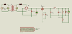
If by peak voltage at output of bridge is 270*1.4142 = 382V then does that mean that if I need 15V output then remaining voltage drops across inductor and Mosfet ? If yes, what will be the approx voltage drop across Mosfet drain to source ?

C1 is 1000 uF 50V

Bridge is 1kV 35A type (GBPC3510

C2 is 330uF 400V Electrolytic.

Circuit is attached.

Document I am referring is also attached.

Also to run a PIC and the IR21xx device I need 5V and 12V. How to get these voltages ? From 12V battery ?
 

Attachments

  • IZWAN_BIN_CHE_SHAM.pdf
    1,021.5 KB · Views: 182
  • Buck Converter.PDF
    29.7 KB · Views: 182

What is the problem in schematic ? I am new to Buck Converter design. Earlier I tried to design a SMSP (transformer based) Battery charger but it included a transformer and to reduce cost I am designing Buck Converter.

I am only testing in Proteus for now. If everything works fine then I will build the hardware and test it.

According to you what will blow up in my circuit ?

As I am testing in Proteus I am safe. You can tell me what changes I have to make.
 

First you will blow up the BR1 diode bridge when you will connect it to AC power with uncharged C2. Than C2 will be blowed up because of AC current that will come throught destroyed BR1. At the same moment n-channel mosfet Q1 connected as current limitter will be blowed up by high current throught it because too high voltage drop. If you wil survive after that you will be able to see how C1 will blow up last one. Only L1 can survive in this fireshow. Why proteus can't simulate fire? Calling to 911? Medical threathment?
 
  • Like
Reactions: badea

    badea

    Points: 2
    Helpful Answer Positive Rating
Why do you say bridge explodes ? What is the problem. I am using 330uF 400V Capacitor at the output of the bridge as a resorvoir capacitor and also to smooth the ripples. Bridge can handle the voltage and current.

Which Bridge Rectifier can I use for my design ?
 
Last edited:

Then what is the problem ? In the document in post #1 how did he designed the buck converter ? What is the difference between his circuit and mine ?

This is the latest circuit. Mosfet I have choosen 900V type. Some 315V drop across Mosfet. What is the problem ? It is well within the limits. See attached file. It shows the voltages.

- - - Updated - - -

@EasyRider83

Do you say this also explodes ?

https://microcontrollerslab.com/buck-converter-using-pic-microcontroller-ir2110/


In the attached document he is using these components. How are they different from my circuit ?

A Datasheet of PIC18F4550 59
B Datasheet of IR2109 half bridge driver 63
C Datasheet of IRF740A SMPS MOSFET 68
D Datasheet of LM7805 series voltage regulator 70
E Datasheet of LM7a15 series voltage regulator 70
F Datasheet of 15ETL06FPPPbF ultra-low
VF hyper fast rectifier 73
G Datasheet of KBPC2510 25amp silicon bridge rectifier 75
H Datasheet of 4N25 optoisolator transistor 76
I Circuit schematic of the Buck converter project 78
J Source code 81
K List of components 82


I found this nice article.

https://www.learnabout-electronics.org/PSU/psu31.php

Why do you think my circuit explodes ? What is the reason ?
 

Attachments

  • Buck Converter.PDF
    36.8 KB · Views: 116
  • SITI_JAMILAH_MAHFUL_2.pdf
    3.1 MB · Views: 133
Last edited:

Problem is that you don't feel the difference between high and low side transistor switching. You just simply connecting gate to driver without understandig how exatly it should work. That's why I don't wanna help you much. You don't want to think, you want to play proteus and expect that in real life everything will work the same.
 

I am sorry Okada but....your schematic does have many fatal errors.

Like easyrider83 mentions, the way you are connecting the Mosfet driver to the Mosfet itself is incorrect.
1- You are driving a high side switch from a low side output, for starters.
2- There is no bootstrap capacitor nor diode.
3- R2 is pulling the gate to ground. If C1 holds any charge you could exceed Vgs(max) and blow the Mosfet.
4- The microcontrollerslab link that you provided talks about converting from 12v to 5v. You are planning to convert from 382v to 12v.
5- The attached .PDF files are heavy on theory and ultra-light on practical advice. Do you know how to prevent high current ground loops? How to prevent inductor saturation? I don't think the author actually built a physical circuit. If he had done so, he would have attached actual scope waveforms, plus some real performance data: line and load regulation, efficiency, ripple voltage.
6- There is no current sensing and therefore no current limiting
7- Using a 28 pin, microcontroller does not make sense where a 8 pin device could be used.
8- There is no feedback loop compensation.
 

Now is the circuit Ok ? I have modified the circuit. Diode I am not still sure what rating I have to use. Check the Mosfet and Mosfet Drive circuits.

Actually I was thinking about using Logic Gate Mosfets which could be driven from PIC directly or through 4N37 and hence did not give much importance to FET Driver circuit. As there was no Logic Gate Mosfet in Proteus I had used FET driver.

I am using 28 pin PIC but later I can change it to 18 pin or 14 pin PIC because I want to use 20x4 LCD. The Buck Converter will be a part of the battery charger. The LCD will display Battery Voltage, Current, etc...

If it was only a buck converter then I would have used PIC12F1840.
 

Attachments

  • Buck Converter.PDF
    31.7 KB · Views: 127
Last edited:

Befor giving up can you tell what is wrong in this new circuit ? I have used High side low side driver to drive the mosfet. FET driver connections are correct ? Then what else is wrong ? The 10k resistor from gate to source ?


If output of the buck converter is shorted then inductor L2 will short and open.
 
Last edited:

I think Easyrider gave up. What should I do ? :thinker:

I need to design a 12V to 5V buck converter and a

12V to 5V and 24V buck boost converter.

Nobody told what is the problem in my circuit ? Is it the Inductor ?

Actually I didn't decide the value of the inductor. I have to do the calculations for it. All I know is I have to use a 30A or 40A type ferrite core inductor because I need 20A for charging 200Ah battery.
 

I need to design a 12V to 5V buck converter and a
12V to 5V and 24V buck boost converter.
Nobody told what is the problem in my circuit ? Is it the Inductor ?

Not true, I gave you a long list of issues with your circuit.
Also on your first post you are asking assistance and showing a high voltage to 12 volt buck converter, which is different from your later requirements.

Let me give you my advice:
The problem you have is you are attempting to climb the Everest before having ever climbed even a small mountain.

-Switchmode power supplies are similar to mountain climbing. You need to start small, really small, and learn the techniques required for SMPS design. My first design that actually worked was a 12v to 5v, 500 mA buck converter.
-Read app notes from Texas Instruments, STMicro, ONSemi and others. App notes provide practical advice on switchmode design and construction, with just enough theory such that you understand what is going on.

I'm not attempting to discourage you. But again, using the mountain climbing example, if you do not know what you are doing with a high-power SMPS, you can and will do a lot of harm and damage to yourself and others.
Start with small power, start with an isolated source.
Use off-the-shelf, ubiquitous and proven controller ICs.
 

The main problem with low power design (smps) is actually the switching transformer. This is not my office work. I am designing this for home use and it is difficult to get transformer wound. Nobody is willing to wind 1 or 2 transformers. They say minimum order of 50. I also purchased ETD39, ETD49, ETD44 ferrite cores from ferroxcube and also boobins and copper wires and copper foils but I don't know how multi-tapped transformer is done.

Actually I want to design a high voltage hih current (20A or more) 180V to 300V AC to 325V DC buck-boost converter to get VBUS voltage for my Stabilizer cum Inverter.

And I also need a 180V to 300V AC input to 14.4V DC 20A buck converter for battery charging.

These I need for the same project which is Constant Output voltage Stabilizer cum Inverter.

I realized that I need these converters and hence started this thread.

This is the main thread of the project.

https://www.edaboard.com/threads/361814/

- - - Updated - - -

This is the low voltage circuit I am designing. I still have to calculate the Inductor value and decide the diode and also calculate the feedback voltage divider values.

The mosfet gate can be driven from 5V and hence I have eliminated high-side low-side driver.

Will this circuit work ?

The circuit shows the voltage when mosfet is off.

What diode can I use ? The transformer is 9V 3A type. I need 5V 3A output.
 

Attachments

  • Buck Converter - 12v to 5V.PDF
    29.8 KB · Views: 111
  • NVTFS5811NL-D.PDF
    120.9 KB · Views: 99
Last edited:

@ Easyrider and other Power electronics experts

Is the attached circuit correct ? I have not yet decided Inductor value and Diode. Mosfet I selected for this 15V to 5V buck converter.

These are the calculations. Are these correct. I have referred SITI_JAMILAH_MAHFUL.pdf page no. 21 to 24 (document in post #7) for calculations.

IZWAN_BIN_CHE_SHAM.pdf (post #1)

Mosfet NVTFS5811NL

Buck Converter Input voltage max is 15V

The input of converter can go down upto 20%

that is 20% of 15V is 3V

15 - 3 = 12V

The input can dip upto 12V

Required Output voltage is 5V.

From datasheet of mosfet page no. 2

Determining the frequency range

Dmin = 10%
Dmax = 20%
tr = 55 ns
tf = 40 ns
ton(min) = 10 ns
toff(min) = 20 ns

Inserting in equation gives

4(1 - 0.2) / ((3(55ns + 40ns) + 4(40ns)) <= fswitch <= 4(0.05) / (55ns + 40ns + 4*10ns

3.2 / 445ns <= fswitch <= 0.2 / 135ns

7191 KHz <= fswitch <= 1418 KHz


choosen frequency = 1450 KHz = 1.45 MHz

PWM frequency = 1.45 MHz


This is the code

Code:
unsigned int duty = 0, previous_duty = 0;

void main() {

    CM1CON0 = 0x00;            
    ADCON1 = 0b10110001;        
    ANSELA = 0x01;        
    TRISA = 0x01;    
    PORTA = 0x00;        
    LATA = 0x00;
        
    PWM1_Init(1450000);
    PWM1_Set_Duty(127);
    PWM1_Start();
                
    while(1) {
    
           duty = (unsigned int)ADC_Read(0) >> 2;
           /*
           if(previous_duty != duty) {
                PWM1_Set_Duty(duty);
                
                previous_duty = duty;          
           }
           */   
    }   
}
 

Attachments

  • bc.png
    bc.png
    28.9 KB · Views: 152
  • NVTFS5811NL-D.PDF
    120.9 KB · Views: 100

I am referring the book Power Electronics Third edition by Muhammed H Rashid, page no. 193 for reference.

My Vs(max) is 15V It can dip 3V that is input can vary between 12V and 15V.

Load is 10k

Taking peak-to-peak ripple voltage of 10 mV

Va = 5V

Peak-to-peak ripple current of Inductor is limited to 4A

duty Cycle k = 5/15 = 33.33%

The LC filter values are,

L = 5(12 - 5) / (4 * 1.45 * 10^6 * 12) = 35 / (69.6 * 10^6) = 0.5uH

C = 4 / (8 * 1.45 * 10^6 * 10 * 10^(-3)) = 4.92nF

So, can I choose L = 0.5 uH and C = 4.7 nF ?
 

Your frequency calculations are missing important points like relation of switching frequency and losses. Don't expect that you will make a buck converter with good performance an > 100 kHz switching frequency. But you can try, surely instructive.

Once you think about, you'll also notice that it's effectively impossible to achieve continuous pulse width control with a PIC at MHz switching frequency.

Unfortunately we didn't see yet a working gate driver solution for a NMOS buck switch in this thread, see Easyrider83's previous comments. Using IR2184 high side driver section (post #10) was closest to a solution, but not close enough. All other gate driver circuits simply don t work for a buck converter.

What's the problem with high side bootstrap driver? The circuit requires the switching node (IR2184 pin VS) pulled down to ground periodically to recharge the bootstrap capacitor. Unfortunately that's not guaranteed in an asynchronously switching buck (transistor + diode combination). It can work under specific load and duty cycle conditions but operation isn't reliable.
 
  • Like
Reactions: Okada

    Okada

    Points: 2
    Helpful Answer Positive Rating
Don't expect that you will make a buck converter with good performance an > 100 kHz switching frequency. But you can try, surely instructive.

I will try to design with a 20 KHz PWM.

I just made the calculation looking at that document I mentioned earlier.

Unfortunately we didn't see yet a working gate driver solution for a NMOS buck switch in this thread,

I just referred to this circuit

https://microcontrollerslab.com/buck-converter-using-pic-microcontroller-ir2110/

and made mine.

The only difference I see is that I have a resistor from gate to Vs of FET driver. Is that the problem ?


What's the problem with high side bootstrap driver? The circuit requires the switching node (IR2184 pin VS) pulled down to ground periodically to recharge the bootstrap capacitor. Unfortunately that's not guaranteed in an asynchronously switching buck (transistor + diode combination). It can work under specific load and duty cycle conditions but operation isn't reliable.

I didn't get this. I can't connect Vs to GND because Vs is also connected to source of mosfet and when mosfet is on it will short the +ve bus to GND.
 

I did not tell to short VS to ground. "Pull down periodically" is something different.

Bootstrap drivers are designed to work with synchronous transistor-transistor switchers. They don't work well with asynchronous transistor-diode circuits.
 

Status
Not open for further replies.

Similar threads

Part and Inventory Search

Welcome to EDABoard.com

Sponsor

Back
Top