Continue to Site

Welcome to EDAboard.com

Welcome to our site! EDAboard.com is an international Electronics Discussion Forum focused on EDA software, circuits, schematics, books, theory, papers, asic, pld, 8051, DSP, Network, RF, Analog Design, PCB, Service Manuals... and a whole lot more! To participate you need to register. Registration is free. Click here to register now.

Phase detection mechanism

Status
Not open for further replies.

promach

Advanced Member level 4
Joined
Feb 22, 2016
Messages
1,199
Helped
2
Reputation
4
Reaction score
5
Trophy points
1,318
Activity points
11,636
1) Do anyone know how this https://github.com/promach/DDR/blob/main/phase_detector.v works internally ?

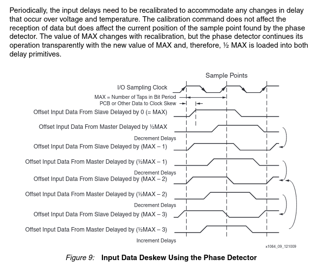
2) What does it mean by MAX in Figure 9 of XAPP1064 appnote ?

3) Could anyone explain what it means by Early Data Sampling and Late Data Sampling ?

4) As for why is it 5 bits wide for pdcounter , someone told me that the verilog code only supports 32 (which is equivalent to 25) steps, but that is 1/8 of the total possible delay steps (256 delay taps) ?
1624022753392.png


1624022766557.png
 

2) MAX = The number of taps to get the delay time equal to the clock period
3) Early data sampling = the sample was taken before a known/expected edge, late data sampling = the sample was taken after a known/expected edge
4) The pdcounter value has nothing to do with the tap number. It is a statistical/averaging counter to avoid unnecessary tap changes.
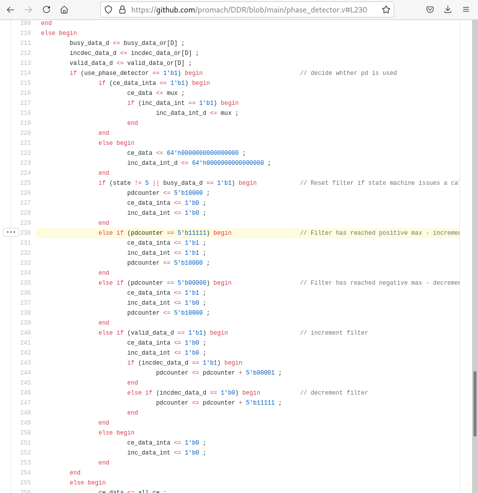
Every "valid" sample (an edge occured) is "early" or "late", so the pdcounter value will always change. When the "early" or "late" samples dominate, the pdcounter will eventually reach one of it's limits, and the master delay will be ordered to change the delay tap.
 

Could you highlighted which exact lines of code are about "the master delay will be ordered to change the delay tap." ?
 

The master delay is adjusted to get samples in the middle of the eye.
The slave delay is adjusted to get samples between the eyes, where the data is expected to change.
Every time the master sampler detects an edge, there is also an edge for the slave, and the slave sample can be detected as "early" or "late", by comparing the sampled value with the master samples, and the pdcounter is incremented or decremented.
When the "early" or "late" has dominated, the pdcounter will reach one of it's limits, and the tap settings will be adjusted, and pdcounter is "resetted" to the middle value.
--- Updated ---

Could you highlighted which exact lines of code are about "the master delay will be ordered to change the delay tap." ?
The order to change tap is "ce_data_inta <= 1'b1 ;"
And the slave tap will also be adjusted.
 
Last edited:

    promach

    Points: 2
    Helpful Answer Positive Rating
Any idea about these few signals ?


Code:
assign incdec_data_im[i] = inc_dec[i] & mux[i] ;            // Input muxes
assign incdec_data_or[i+1] = incdec_data_im[i] | incdec_data_or[i] ;    // AND gates to allow just one signal through at a tome
assign valid_data_im[i] = valid[i] & mux[i] ;                // followed by an OR
assign valid_data_or[i+1] = valid_data_im[i] | valid_data_or[i] ;    // for the three inputs from each PD
--- Updated ---

The order to change tap is "ce_data_inta <= 1'b1 ;"
As for ce_data_inta ,
how is the following code snippet related to changing delay tap ?

Code:
        if (ce_data_inta == 1'b1) begin
            ce_data <= mux ;
            if (inc_data_int == 1'b1) begin
                inc_data_int_d <= mux ;
            end
        end
 

It seems to be code for adjusting several delay lines from the same state machine, but I don't see exactly how it works.
"mux" seems to select the delay line for one data bit at a time, but there is only one pdcounter.
I think pdcounter is adjusted regardless of the selected data bit, but only the delay line for one bit will be adjusted every time pdcounter reaches one of the limits.
 

Code:
[phung@archlinux DDR]$ grep -n IODELAY *.v
phase_detector.v:23://        - State machine changed slightly to enable individual control of INC pins on IODELAY2s
phase_detector.v:67:input    [D-1:0]        busy ;            // BUSY inputs from IODELAY2s
phase_detector.v:73:output            cal_master ;        // Output to cal pins on master IODELAY2s
phase_detector.v:74:output            cal_slave ;        // Output to cal pins on slave IODELAY2s
phase_detector.v:75:output            rst_out ;        // Output to rst pins on master & slave IODELAY2s
phase_detector.v:76:output    [D-1:0]        ce ;              // Outputs to ce pins on IODELAY2s
phase_detector.v:77:output    [D-1:0]        inc ;              // Outputs to inc pins on IODELAY2s
phase_detector.v:140:          if (enable == 1'b1) begin                // Wait for IODELAY to be available
phase_detector.v:156:       4'h2 :     begin                            // Now RST master and slave IODELAYs needed for simulation, not for the silicon
phase_detector.v:168:       4'h4 :     begin                            // Wait for IODELAY to be available
phase_detector.v:193:       4'h8 : begin                            // Wait for all IODELAYs to be available, ie CAL command finished
serdes_1_to_n_clk_ddr_s8_diff.v:70:wire         ddly_m;             // Master output from IODELAY1
serdes_1_to_n_clk_ddr_s8_diff.v:71:wire         ddly_s;             // Slave output from IODELAY1
serdes_1_to_n_clk_ddr_s8_diff.v:95://        IODELAY for the differential inputs.
serdes_1_to_n_clk_ddr_s8_diff.v:97:IODELAY2 #(
serdes_1_to_n_clk_ddr_s8_diff.v:125:IODELAY2 #(
serdes_1_to_n_data_ddr_s8_diff.v:89:wire     [D-1:0]        ddly_m;             // Master output from IODELAY1
serdes_1_to_n_data_ddr_s8_diff.v:90:wire     [D-1:0]        ddly_s;             // Slave output from IODELAY1
serdes_1_to_n_data_ddr_s8_diff.v:145:IODELAY2 #(
serdes_1_to_n_data_ddr_s8_diff.v:172:IODELAY2 #(
[phung@archlinux DDR]$

@std_match the whole purpose of the phase_detector.v is used to control CAL pin of the IODELAY2 primitive
 

@std_match the whole purpose of the phase_detector.v is used to control CAL pin of the IODELAY2 primitive
Yes, but it wasn't clear how multiple data lines are handled. It looks like the state machine "slowly" moves from pin to pin and adjusts the corresponding master and slave IODELAY2 primitives. "mux" is a one-hot register with a '1' for the data path that is currently being adjusted.


The "master" is used for the actual data sampling. The delay is adjusted so the sampling is in the middle of the eye.
The "slave" is used for the continuous delay adjustment. The delay is adjusted to be where the data is expected to change.
Every time there is an edge on the data (= the data bit changed), is is checked if the slave sampled the old or the new value (early or late sampling).
When early or late dominates, the pdcounter will eventually reach one of it's limits, and both ISERDES2 primitives are ordered to increment or decrement the delay by one tap.

The master can't be used for the timing adjustment, because the need for a delay change wouldn't be detected until the data had already been corrupted.
 

    promach

    Points: 2
    Helpful Answer Positive Rating
@std_match What do you exactly mean by "The master can't be used for the timing adjustment, because the need for a delay change wouldn't be detected until the data had already been corrupted." ?
 

@std_match What do you exactly mean by "The master can't be used for the timing adjustment, because the need for a delay change wouldn't be detected until the data had already been corrupted." ?
I mean that if we only look at the data samples that we want to take in the middle of the eye (the position is determined by the "master" delay line), there is no way to detect that the sample point drifts away from the middle of the eye.
The drift of the sample point is controlled by the "slave" delay line. It is adjusted to get another sample from the same data line, with the worst possible timing, exactly where the data value is expected to change. Every time a transition is detected by looking at the "master" samples, there will also be a transition in the "slave" samples, but we don't know in advance if the slave sample will be taken before or after the transition (early or late). By comparing the master samples and the slave sample, it can be determined if there was a transition, and if the slave sample was early or late. pdcounter counts up or down when there is a transition, depending on the early/late decision. If there are too many of either "early" or "late" samples, the slave sample isn't taken at the optimal position, which also means that the master sample isn't taken in the middle of the eye. This is corrected by adjusting the tap position in both the master and the slave delay lines whenever pdcounter reaches one of it's limits.

The occasional calibration is needed to calculate the number of taps that corresponds to one bit time (= MAX), so that the slave delay can be set to sample half a bit time earlier than the master (= MAX/2 number of taps earlier).
 
Last edited:

    promach

    Points: 2
    Helpful Answer Positive Rating
I have a feeling that this dynamic phase calibration would only work well with two assumptions:

1. needs some clock cycles to use the data delay information to do deliberate phase adjustment
2. there has to be enough bit transitions for the incoming data bits

Please correct me if wrong
--- Updated ---

Would using bitslip be more suitable in this case ?
1) Yes, this is done by the calibration mechanism inside the IODELAY2, and takes 8-16 GCLK cycles.
The data is invalid during the first calibration, but subsequent ones can be made without disturbing the data reception by only calibrating the slave delay, and setting the slave sample point the new MAX/2 taps earlier than the current master sample point. It is assumed the the master and slave delays are similar for a certain tap setting.

2) Yes, this is always true when you want to extract the sample clock from the data itself. Transitions can be guaranteed by using 8b/10b, 64b/66b coding or similar.

Bitslip) As I understand the "bitslip" block, it has an input clock, and can only move bits in clock period steps. You can't do the sub-bit fine tuning that the taps in IODELAY2 can do (Xilinx uses 40 ps as an example value for the delay per tap).
 

    promach

    Points: 2
    Helpful Answer Positive Rating
Thanks for your explanation.

The data is invalid during the first calibration

Why invalid ?

Transitions can be guaranteed by using 8b/10b, 64b/66b coding or similar.

Not all signal protocols are using such encoding scheme. One example would be DDR3 RAM data protocol. So, this dynamic phase calibration would not work for all kinds of signal protocols. Please correct me if wrong.


By the way, someone told me the following regarding the difference in purpose between bitslip (1-bit shift which is equivalent to nano-second shift) and IODELAY2 (pico-second shift)

so the vaguely general description is that variations in things like PCB trace length can lead to variable amounts of skew between periodic (K clocks) or strobe (dqs) signals, such that the rising edge of these signals may not match up well with the data to be sampled. So, during DDR calibration you're going to first perform fine-tuned adjustment of the IODELAY taps in order to center the clocks/strobes between transition edges of your data. However, because the IODELAYs can only ...well, delay things...it's possible that the clocks/strobes can end up centered but a cycle out of sync. So the bitslip provides a way to delay the incoming signals on a cycle by cycle basis to account for that.

Now reading the bitslip appnote for actual coding implementation leads to some Solution A and Solution B ?
 

Although DDR3 interface use dynamic phase calibraton, the application notes referenced in this thread (XAPP1064, bitslip AN) are not related to DDR interfaces as far as I'm aware of. The DDR interfaces I have yet worked with are calibrating with dedicated test data written to DDR RAM and read back. High speed serial transmission protocols have always balanced bit streams and thus guaranteed transitions.
 

    promach

    Points: 2
    Helpful Answer Positive Rating
@FvM So, this dynamic phase calibration would not work for DDR RAM interface protocol during real-time (not the initial ZQCL command) data reception. Please correct me if wrong.

Note: DDR RAM interface protocol is not using 8b/10b, 64b/66b coding or similar.


@std_match Why the data is invalid during the first calibration ?

For bitslip, Figure 6 and 7 from Solution A seems only rotated the data bits. What effect does this have ? How is Solution B different from Solution A ? Which solution variant is recommended ? and why ?

1624626761339.png
 

First, we are discussing two separate things here.
The "phase detection" is about sampling the input data at the right moment, to get the data bits.
To reduce the clock rate needed for processing the data, the serial data bits are converted to parallel by a serial-to-parallel shift register.
The serial-to-parallel shift register doesn't know where the serial words begin or end, so it is likely that the output words contain data from two words in the serial stream. This can be corrected by the "bitslip" function.

For the phase detector, the data is invalid during the first calibration because the tap setting in the master IODELAY2 is not correct until the calibration is complete, which means that it is possible that some input bits weren't sampled at all. "invalid" = don't use the bits because they may be wrong

The bitslip function is not only a rotation. When active, each output word will contain data from two different input words, to compensate for the misalignent in the serial-to-parallel converter. It is just luck if the output from the shift register is the "real" words in the serial stream. Most of the time, the bitslip function is needed to align the words.

Solution A only produces one possible alignment at a time, so it can take some clock cycles to get it right. Some other logic must detect if the alignment is correct or not, and tell "solution A" to change the bitslip.

Solution B produces all possible alignments every clock cycle, so it can be used to detect a sync pattern in the input data and immediately produce words with the correct alignment. So solution B is faster but needs more resources since one comparator for each possible alignment is needed to detect the sync pattern.
 

    promach

    Points: 2
    Helpful Answer Positive Rating

You are trying to connects subjects that aren't related.
The "phase datector" is used to sample bits in the middle of the eye, to maximize the probability that the correct value is sampled.
The "bitslip" is to align bits after they have been sampled.
You have also asked about two different bitslip situations. In post #13 it is about aligning words after a serial-to-parallel conversion.
This is handled by shifting bits so the output words correspond to the words in the serial stream.

In post #19, the bitslip is about aligning several parallel streams to each other. It is just a delay adjustment for each individual bit, in pictures 17-21 to 17-23 (here the delay is changed complete bit times, not like the sub-bit delay adjustment in the phase detector).

The situation is very different between high-speed serial interfaces and DDR memory. For DDR memory you have a clock that is phase locked to the data bits (but the phase relationship can drift a little during operation). I think the code in your phase_detector.v is only needed when you don't have such a clock.
 
Last edited:

    promach

    Points: 2
    Helpful Answer Positive Rating
Status
Not open for further replies.

Part and Inventory Search

Welcome to EDABoard.com

Sponsor

Back
Top