Continue to Site

Welcome to EDAboard.com

Welcome to our site! EDAboard.com is an international Electronics Discussion Forum focused on EDA software, circuits, schematics, books, theory, papers, asic, pld, 8051, DSP, Network, RF, Analog Design, PCB, Service Manuals... and a whole lot more! To participate you need to register. Registration is free. Click here to register now.

PCB Testpoint strategy for 100 MHz digital signals

Status
Not open for further replies.

gemass

Newbie level 3
Newbie level 3
Joined
Nov 10, 2011
Messages
3
Helped
0
Reputation
0
Reaction score
0
Trophy points
1,281
Activity points
1,303
Hello everyone,

I'm new to PCB design and currently designing my first 2-layer board.
I have digital output signals having a frequency ranging from 50 to 100 MHz that I would like to probe. What is the best test point strategy to not loose the shape of my signal ?
Are surface mount test point good for that ? (for example: https://www.keyelco.com/products/prod...CategoryID=113)
Is it better to use a via without solder mask on it or just a big pad and solder a wire to probe on it ?

Thanks a lot for your help !
 

The properties of the probe itself is probably more critical for things like this. For example most standard probes have >10pF of loading capacitance, which can be very significant for high speed digital. Special digital probes are much better.

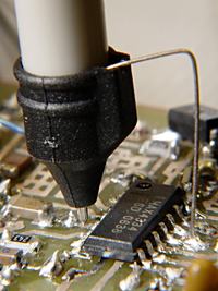
If you have to use standard probe, then you should use a "pig tail" ground lead on the probe, as shown in this image here:


So for the layout, all you want is a pair of plated holes/vias, one for the probe tip and one for ground. Just space them apart appropriately so the probe fits easily into them (usually 5-10mm).
 

At these higher frequencies you are better of using a probe with the return lead as close as possible to the probe tip as possible, even the length of the ground shown above will add more loading than you want affecting the signalyou see. The Tek site in the first link has some very good information. I have download and moddeled quite a large number of both Tek and Agilent probes, so that when doing signal integrity verification I can load the line with the scope probe parasitics and thus see on screen the same wave as shown on the scope.
http://www.tek.com/application/signal-integrity

http://www.sigcon.com/Pubs/straight/probes.htm

http://www.eevblog.com/forum/beginn...und-lead-length's-affect-on-signal-integrity/
 

Status
Not open for further replies.

Part and Inventory Search

Welcome to EDABoard.com

Sponsor

Back
Top