lfx0828
Newbie level 4
Hi all,
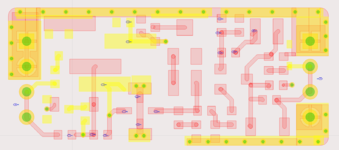
Recently, I am trying to do EM simulation of a 2-layer PCB in ads.
Unfortunately, the result is not correct, it seems there is an open-circuit for the non-ground via.
As shown in the attached image, the DC properties on the top layer is correct, but on the bottom layer is wrong.
The project file is also attached.
Any help will be fully appreciated!
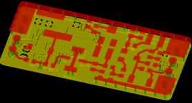
Attachments
Last edited by a moderator: