useless018
Junior Member level 1
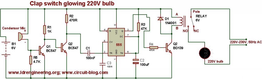
hello everyone,,,
can someone help me in making the PCB layout for this clap switch schematic diagram,,,,,
i've not tried it yet,, so i dont know if it is working kindly check the circuit thanks ^_^
**broken link removed**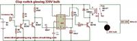
---------- Post added at 15:01 ---------- Previous post was at 14:55 ----------
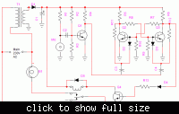
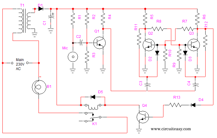
heres the other circuit ^_^
can someone help me in making the PCB layout for this clap switch schematic diagram,,,,,
i've not tried it yet,, so i dont know if it is working kindly check the circuit thanks ^_^
**broken link removed**
---------- Post added at 15:01 ---------- Previous post was at 14:55 ----------
heres the other circuit ^_^