bio_man
Full Member level 2
Hi,
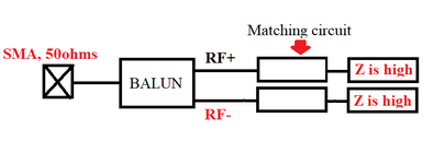
I want to design a PCB circuit that receives 1GHz from an antenna through SMA connector and convert the RF signal to differential outputs RF+ and RF-.
Basically, I have SMA connector (50ohms) followed by BALUN (to provide differential output signals: RF+ and RF-), PCB will be fabricated using FR4 material.
The issue I'm facing, most of the BALUNs are primary/secondary, I can't find ones that have a secondary side with center tapped to provide RF+ and RF-
Any suggestions with this regards?