Continue to Site

Welcome to EDAboard.com

Welcome to our site! EDAboard.com is an international Electronics Discussion Forum focused on EDA software, circuits, schematics, books, theory, papers, asic, pld, 8051, DSP, Network, RF, Analog Design, PCB, Service Manuals... and a whole lot more! To participate you need to register. Registration is free. Click here to register now.

PCB layers

engr_joni_ee

Advanced Member level 3
Joined
Nov 3, 2018
Messages
750
Helped
2
Reputation
4
Reaction score
4
Trophy points
18
Activity points
6,229
Hi, I have some questions regarding PCB layers.

There are two types are dielectric layers between copper layers. They are called prepreg and core materials. In a two layer board which dielectric do we have in between top and bottom copper layers, is that core or prepreg ?

I read that cores are copper clad-laminates and they are fully cured and their thickness does not change after the lamination. But prepreg are semi-cured and they used as bonding material between two core laminates given that both side of core are copper layers. After lamination the height of the prepreg change which canbe seen in attached stakup.

How the final thickness of the prepreg changes in manufacturing, some explanation please ? The core height remains the same. How about the copper height ? does it remain same in final production ?

I also don't understand how the first dielectric under the top and bottom copper layer is prepreg ? The PCB layers are staked using core with copper on each side then how we can have prepreg under the outer copper layer ?

And how the percentage of copper is changing in the inner layers and not on the outer layers ?
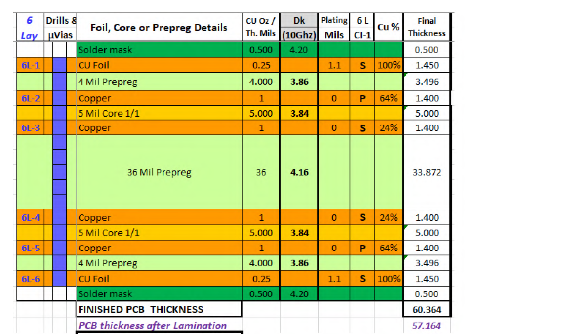
1700733470024.png
 
Two layers:

bottom copper - core - top copper.

If I´m not mistaken: (please someone correct me if I´m wrong)
The PCB manufacturer buys
* [copper - core - copper] with variable core thickness ... as one thing
* [prepreg] in variable thickness to be laminated at the PCB manufacturer
* [copper foil]

--> for a 2 sided PCB .... they just use what they have bought and don´t laminate at all.

--> for your 6 layer as shown above they use
[copper foil]
[prepreg] ...to be laminated
[copper - core - copper]
[prepreg] ...to be laminated
[copper - core - copper]
[prepreg] ...to be laminated
[copper foil]

thus the "core" is fully cured, while the "prepreg" layer is cured during PCB production and may post cure (change mechanical and electrical characteristics)

Klaus

Added:
You may do an internet search on "PCB production" or "what is the difference between prepreg and core" on your own.
The internet is such a useful source of information.
 
Thanks again for reply. This means the fabrication house have three type of items to place in the PCB stackup.

1- [copper foil]
2- [prepreg]
3- [copper - core - copper]

They can take the fully cure material first, which is [copper - core - copper] then they apply [prepreg] and then place [copper foil] as top layer and press and cure thermally, right ?
--- Updated ---

Thanks again for reply. This means the fabrication house have three type of items to place in the PCB stackup.

1- [copper foil]
2- [prepreg]
3- [copper - core - copper]

They can take the fully cure material first, which is [copper - core - copper] then they apply [prepreg] and then place [copper foil] as top layer and press and cure thermally, right ?
 
Hi,
They can take the fully cure material first, which is [copper - core - copper] then they apply [prepreg] and then place [copper foil] as top layer and press and cure thermally, right ?
at least this is how I learned it .. but it was many years ago.

Klaus
 
Cores are etched before pressing the layers. The voids are filled by prepreg resin, therefore prepreg thickness decreases more if less copper remains. Final thickness can be found by a simple volume calculation. Top/bottom foil is etched after multilayer assembly, thus outer copper fill factor doesn't affect PCB thickness.
 
In this image, it is a 6-layer PCB with two cores, each core having two copper layers. Between the two cores, there is prepreg with 36mil thickness, which should be a few layers of prepreg and FR4 material bonded together since the stand thickness of prepreg is around 3-8mils.

4mil prepregs are used between the top copper/bottom copper layers to the next layers to bond the outer copper layers with the inner layers and also form a dielectric. The thickness of the prepreg and copper thickness should be the final thickness, as the PCB manufacturer will consider the copper trace density and use proper prepreg in production.
 
Design rules for core prepreg have many variables;
- mainly used as a bonding agent,
- also impedance, UHF losses (Tan δ or Df) , Glass/(Glass+Resin ), ratio, % Resin, tensile | flexural strength, thermal k, Tg, CTE,
- cured cores are for bulk strength with stable thickness also better for highest f controlled impedance corrections
- outer Cu layer can be any thickness + same in plating thickness or immersion gold etc + mask, 35.6 um = 1.40 mils / "oz" for Cu or plating

- power level, trace resolution, differential depends on or crosstalk , balance, coplanar or dual stripline on core (best but $ if low fill)
- in high volume std. FR-4 $ depends on cost of Cu content then cost factors rise rapidly for low Tan δ and complex drill/mill, BBV

- dielectric loss tangent (tan δ) required which affects Er = εR = (epsilon R = relative permittivity) aka Dk (dielectric constant)
- choices of dielectric constant (hi/lo) other than std FR-4 which affects $ PTFE(Teflon) is Er=2.1 , AlO2(Alumina) = 6.1 , ceramic-PTFE hybrid Er=10

more info https://www.protoexpress.com/pcb-design-guides/pcb-material-design-guide/

Sperry plant in Bristol TN, USA used to make 50 layer PCB's for their mainframes until closed in 80's. The also employed 2 Chemists to control the process and contaminant levels (antimony etc) , Each acid and rinse bath bigger than dumpsters :cool: and one filled with liquid gold cyanide. Microvia arrays looked finer than an electric shaver foil all with water cooled CPU's. Korean Co. bought it with 200 ksqft and took the gold and never did what they promised to create jobs.
 
Last edited:

LaTeX Commands Quick-Menu:

Part and Inventory Search

Welcome to EDABoard.com

Sponsor

Back
Top