Continue to Site

Welcome to EDAboard.com

Welcome to our site! EDAboard.com is an international Electronics Discussion Forum focused on EDA software, circuits, schematics, books, theory, papers, asic, pld, 8051, DSP, Network, RF, Analog Design, PCB, Service Manuals... and a whole lot more! To participate you need to register. Registration is free. Click here to register now.

PCB Foorptint Query (Top Solder)

Status
Not open for further replies.

sakibnaz

Full Member level 3
Full Member level 3
Joined
Jul 6, 2008
Messages
165
Helped
6
Reputation
12
Reaction score
6
Trophy points
1,298
Activity points
2,778
Hi.

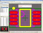
I am using a MSOP-8 PCB footprint. I can see the Pads are very close where Top Solder of Pad are touched with other Pad.

I am worried ... will it make problem (Pads will short together) after production of PCB???

Please see the attached image.

I am took this Footprint from Altium Microchip Lib.

Thanks in advance.

Regards.
 

Attachments

  • PCB_Footprint.JPG
    PCB_Footprint.JPG
    218 KB · Views: 115

If this is a standard library part you might hope that it won't be a problem.
Your picture looks like the purple touches but I would expect that to be the solder resist layer, it's much more likely the red are the copper pads.
You might be wise to check the chip datasheet for the correct pad layout.
Your pcb manufacturer will have a minimum pad separation that you can check against, 0.1mm is usually available but will be the most expensive.
 

it is top solder mask, it will not effect ur connections. don't worry
 

Yes it does matter, you are likely to get solder bridging during production on this part, you need a solder dam between the pads on such small devices. Look up IPC-7351 footprints or change the pad size and solder mask opening for the footprint you have.
 

There are different MSOP packages in the Altium designer PCB libraries.

The first point is to check if 0.45 pad width is appropriate for the respective part. It might be for some power devices that have relative wide pins.

Secondly, the solder mask finish depends an actual expansion rules. Now it's apparently about 0.1 mm, which mostly isn't acceptable for high density boards. They require 0.075 down to 0.05 mm.

There's however a minimum solder mask width that can be reliably structured. Below this value, solder mask strips might break and foul the PCB surface, particularly SMD pads.

So all in all, it depends on available PCB technology. With low technology, it may be necessary to omit any solder mask feature between small pads, despite the risk of solder bridging.
 
Change your solder mask so that it is 1:1 and not oversized.

While historically pcb designers would oversize their solder resist it is now better to leave it at 1:1 and allow the PCB manufacturers to oversize it according to their manufacturing requirements.

All you need is the simple instruction that there should be no solder resist on pads (which is standard).
 

The large pads are not required to form a reliable solder joint, with surface mount production there is no low technology, its either done right or its not, ie you place the parts and reflow them, when you get down to components this size you have to use the correct paste with the right size balls for the stencil opening etc.
Having been involved heavily in SMD production for many years, one of the biggest problems with solder mask blocking is solder shorts during production, a solder mask dam stops this, you should be able to get a 0.1mm dam between those pads. This is thye cheeper option than reworking lots of boards because of solder bridging.
 

Status
Not open for further replies.

Part and Inventory Search

Welcome to EDABoard.com

Sponsor

Back
Top