kotshe
Junior Member level 3
Hi All ,
I'm trying to set Differential Pairs Impedance at 90 Ohm's For standard PCB FR4 of two layers , i'm trying to use Saturn PCB design , what I can't understand what is conductor Height .
I have
Base copper Weight = 18um
Plating thickness = 18um
Er = 4.6
But I cant understand what conductor Height is ?
Any help please
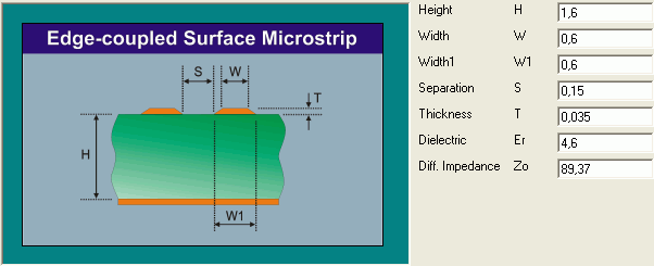
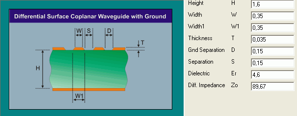
") (Zo = 55OHMs, Zdiff = 90OHMs)
(Zo = 55OHMs, Zdiff = 90OHMs)