Continue to Site

Welcome to EDAboard.com

Welcome to our site! EDAboard.com is an international Electronics Discussion Forum focused on EDA software, circuits, schematics, books, theory, papers, asic, pld, 8051, DSP, Network, RF, Analog Design, PCB, Service Manuals... and a whole lot more! To participate you need to register. Registration is free. Click here to register now.

[SOLVED] PCB Design: How fast data rates with pin headers?

Status
Not open for further replies.

TommiRouvali

Junior Member level 1
Joined
Mar 9, 2012
Messages
18
Helped
9
Reputation
18
Reaction score
9
Trophy points
1,283
Visit site
Activity points
1,422
Hi,

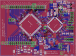
I designed PCB with Spartan 6 FPGA and my plan is to stack this board with other board having AD or DA converter (like AD9744). I was wondering how fast data rates are possible with pin headers like this: https://www.pololu.com/catalog/product/965 .(and female connectors matching it)

I know there is no simple answer, it depends on line impedances, connector quality, driver and receiver properties and so on. But I imagine someone with more experience can say is 50Msps, 100Msps or 200Msps I can use to drive DA converter?
SpartanBoard.png
 

200 MSPS isn't a problem with 0.1" headers as such, but for the present development board, single ended IO without sufficient ground connections will result in poor signal quality.
 
What you need to do is to "slow-down" the drivers of your digital signals. In other words, if you can, set the rise/fall times of your drivers to a maximal value for your digital bitrate. If possible, use differential signaling instead of single ended ones.
 
FvM: So you suggesting I should add more ground connections to headers. For example each other pin, or at least few to center?

If you were referring to bottom layer ground plane(blue), there are 0 ohm resistors to make ground more solid.
 

So you suggesting I should add more ground connections to headers. For example each other pin, or at least few to center?
Yes.
If you were referring to bottom layer ground plane(blue), there are 0 ohm resistors to make ground more solid.
I'm referring to the pin header assignment. Feasibility of 200 MSPS FPGA-IO on a two-layer PCB is beyond the original question, I think.

I'm not so familiar with Xilinx FPGA, but generally I would rate it as experimental layout, with a certain chance to get it working.
 
Status
Not open for further replies.

Part and Inventory Search

Welcome to EDABoard.com

Sponsor

Back
Top