Continue to Site

Welcome to EDAboard.com

Welcome to our site! EDAboard.com is an international Electronics Discussion Forum focused on EDA software, circuits, schematics, books, theory, papers, asic, pld, 8051, DSP, Network, RF, Analog Design, PCB, Service Manuals... and a whole lot more! To participate you need to register. Registration is free. Click here to register now.

passing absolute maximum rating of JFets

Status
Not open for further replies.

fala

Full Member level 5
Joined
Sep 18, 2005
Messages
249
Helped
19
Reputation
38
Reaction score
4
Trophy points
1,298
Activity points
3,569
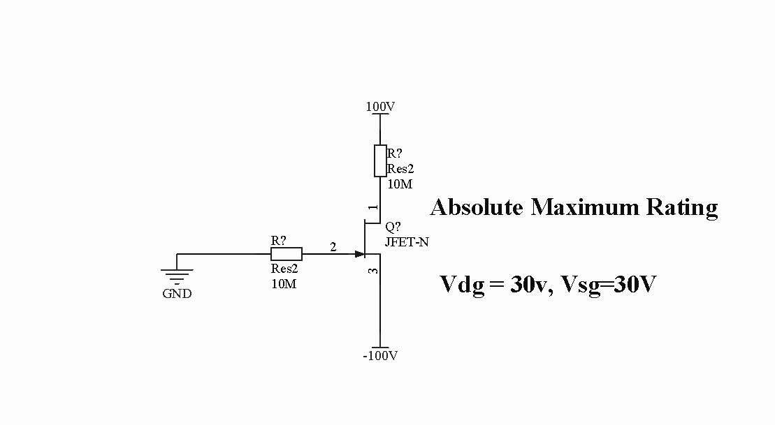
Hello board, I want to know if I can pass safely absolute maximum rating of Vds, Vgs, Vds of JFETs safely provided that current is limited? eg. 100V for a JFET that has 30V absolute maximum rating, but voltage will drop below 30V if a few uA current is drawn.
 

every device has its own characteristic resistance and other parameters.... when you apply 100V across the JFET then it has to satisfy the V=IR eqn also... do you think a MOSFET resistive enough.... also 100V maybe high enough to cause breakdown.... always specs about max rating would have some conditions specified....
if it could have been exceeded then the company would have done that and put that in the datasheet na!!!!

also one important thing is that these specs are just approximations,,,.. a JFET may fail below that specified value too....
 

Let's talk by an example, For example this:
 

that circuit would surely burn out... the gate source terminal would burn out because the voltage across it is too much....
 

Anand, Why? how you are so sure? how a few uA can burn source gate diode??? can you explain about the reason, please?
 

when you keep increasing the voltage difference the charge carriers gain enough energy to cross the barrier between the gate and the source... this would lead to more and more charge carriers and hence effectively the current increases and the circuit burns out...

how much potential do you expect the gate source terminal to bear....
 

Anand potential difference can't destroy anything, it is the flow of electrons that causes destruction. I completely agree that energy barrier will be passed and electrons will start to flow but before the current flows become destructive it will be limited to maximum a few uAs and I really can't understand how a few uA can destroy a diode???
 

electrons get attracted due to potential... and using this energy due to the potential only they cross the barrier....
have you heard of the term avalanche breakdown... that is what would actually happen.. actually this current is flowing across a reverse biased diode and 100V is too much of energy and hence each electron on its way is going to induce more electrons to flow...
this leads to a lot of heating and maybe hotspots would form due to the heating and once these are formed the resistance drops just like that and after that you cant be talking in µA.... the current would be very high and the device would be permanently damaged...

hope u understand this... else point to which part you dont understand...
 

Hello anand, I know about avalanche breakdown but there is another important law called kirchoff current law that says the total charge that flowing out of a node must be equal to the charge flowing into a node. can you tell me from where current in excess of a few uA will enter the gate source node?
 

dude you have connected a -100V source... it can source all the current that is needed... once the barrier is broken the source is at its legacy to supply very large current and satisfy the kirchoff law you are talkin about.... once the barrier is broken the resistance is very low than before and large current flows and leads to avalanche effect.... and hence to burn out...
 

Anand, Even if we assume source gate resistance becomes zero due to avalanche effect that you mentioned, there is a 10M resistor between -100V and ground so at most it will draw 10uA, which causes the voltage to drop to -100V across 10M resistor so source and gate will have the same potential. -100V can't source current to nowhere land!
 

k... now i get you... so speaking in that term suppose a current around 10µA is flowing then it is also flowing through the 10M to so you are having around 100V drop across the resistor and hence you are subjecting the MOS to a voltage very very less than the rating you have specified... which is totally deviating from what you wanna know...
 

    fala

    Points: 2
    Helpful Answer Positive Rating
Anand, It is not totally deviating from what I want to know in the original post I have asked
" I want to know if I can pass safely absolute maximum rating of Vds, Vgs, Vds of JFETs safely provided that current is limited? eg. 100V for a JFET that has 30V absolute maximum rating, but voltage will drop below 30V if a few uA current is drawn. "
 

fala said:
Anand, It is not totally deviating from what I want to know in the original post I have asked
" I want to know if I can pass safely absolute maximum rating of Vds, Vgs, Vds of JFETs safely provided that current is limited? eg. 100V for a JFET that has 30V absolute maximum rating, but voltage will drop below 30V if a few uA current is drawn. "

when you mean safely pass Vds and Vgs rating it means the voltage across the drain source terminal and gate source terminal

i accept you have current limited the circuit....
but now you are talking about gate source terminal plus a resistor...
i think you can understand what i'm saying...
 

    fala

    Points: 2
    Helpful Answer Positive Rating
Status
Not open for further replies.

Similar threads

Part and Inventory Search

Welcome to EDABoard.com

Sponsor

Back
Top