ranran19870222
Newbie level 6
Hi,
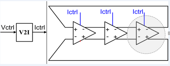
I am working on the design of a delay-line ring oscillator which is composed of three differential delay stages as shown in the pic. My center frequency in the schematic design is 1GHz. I laid it out and got the extracted view. The post-layout simulation gave me a much slower performance (750MHz center frequency). I've looked at the netlist for the extracted circuit, and saw that parasitic caps, resistors, and diodes were added after the extraction. I tried to put the same size caps and diodes into the schematic to check which one caused the problem and found that the parasitic caps are really small and did not affect the performance. However, once the parasitic diodes are added at outputs of each delay-stage (it is where they are in the extracted view), my oscillator starts to get slower.
Is it because the reverse biased parasitic diode capacitance makes the circuit work much slower since the outputs of each delay stage is suppose to be the high speed lines? If that is the case, is there any method to minimize this diode parasitic in the layout?
Many thanks,
Faye