Continue to Site

Welcome to EDAboard.com

Welcome to our site! EDAboard.com is an international Electronics Discussion Forum focused on EDA software, circuits, schematics, books, theory, papers, asic, pld, 8051, DSP, Network, RF, Analog Design, PCB, Service Manuals... and a whole lot more! To participate you need to register. Registration is free. Click here to register now.

Overlap of block hard macro and flip-chip pad

Status
Not open for further replies.

stevenv07

Member level 2
Joined
Aug 11, 2020
Messages
43
Helped
0
Reputation
0
Reaction score
1
Trophy points
8
Activity points
404
Hello everyone,

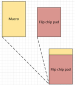
In my design, I have an analog hard macro and its flip-chip pads. Their GDS and LEF files are separate.

I implemented a block design with this macro, its flip-chip pads, and its controller in Cadence Innovus.

Can I place this flip-chip pad over the hard macro in Innovus (see the attached figure)? If yes, could you show me how to place them and the command to do it?

Thanks so much.
Steve.
 

Attachments

  • flipchip.png
    flipchip.png
    11.4 KB · Views: 131

you can if they don't have overlapping layers. this is very typical.
 
Data-on-layer collisions is one thing (bad) but
there is also a question about the qualification status
of pad-over-circuitry. This may be "no", "sure" or
"maybe". The qualification for particular assembly
processes must ensure that (a) the process itself
is in control and (b) across its control range, the
effects of thermal compression bonding (or wire
bonding, variously) are insignificant to any electrical
performance or long term reliability.

In a tall metal stack this is probably not a problem
(plenty of Z crush room) but may or may not have
been proven by a rigorous qualification. If not, you
will have to get customer and foundry waivers to
make product shippable. In few-levels-metal there
is more chance that the violence of assembly process
will alter device attributes through strain effects.
You might find that qualification avoids the subtle
(analog leakage, noise, matching) and just gets you
to where you can put I/O and ESD circuitry under
its associated pad (convenient as this can be
"plugged into" I/O-specific DRC rules, and less
"exposure" to unacceptable results at qual). Or you
may be allowed "digital" but not "analog" circuitry
as small quantities of digital circuitry don't care
about a bit of elevated leakage, or matching and
noise qualities whatsoever.

The foundry should have an opinion, although I
have encountered blank looks more than once on
this question. And it is not just about the foundry,
but your assembly technology and vendor as a
part of that technology mashup.
 

Status
Not open for further replies.

Part and Inventory Search

Welcome to EDABoard.com

Sponsor

Back
Top