Continue to Site

Welcome to EDAboard.com

Welcome to our site! EDAboard.com is an international Electronics Discussion Forum focused on EDA software, circuits, schematics, books, theory, papers, asic, pld, 8051, DSP, Network, RF, Analog Design, PCB, Service Manuals... and a whole lot more! To participate you need to register. Registration is free. Click here to register now.

overlap and width DRC errors in Eagle CAD

Status
Not open for further replies.

electrophile

Member level 2
Joined
Aug 30, 2013
Messages
48
Helped
1
Reputation
2
Reaction score
1
Trophy points
1,288
Activity points
1,677
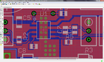
I'm a new Eagle user and I created an SOIC part with a small heat pad in the middle. The pad is on the bottom and at the top copper layers. The bottom pad is purely for soldering convenience sake. Its easy to solder the pad by heating the bottom pad with your soldering iron. Now, the board has 2 layers and the bottom one is all GND. I've attached an image here. The manufacturer says that I should extend the heat pad beyond the IC and put some vias so that heat is transferred to a larger plane. Now I've put these vias and named them GND but I keep getting an "Overlap" error. Why is this? Also all the copper pours are created with zero widths because it gave me better control over the fill and now I get "Width errors". How do I resolve these?
 

Attachments

  • 2013-10-30_140613.png
    2013-10-30_140613.png
    96.9 KB · Views: 80

An overlap error is to be expected when you put vias in the power pads. As long as you are sure the layout is correct you can "approve" then so you don't get them again. I have a board with 117 "approved" errors and some with more than double that.

You don't need zero width to get a good fill and I think it can cause some problems in the Gerbers. Also, the width is used to create the thermals so a sensible size is better.

Keith
 

Status
Not open for further replies.

Part and Inventory Search

Welcome to EDABoard.com

Sponsor

Back
Top