Continue to Site

Welcome to EDAboard.com

Welcome to our site! EDAboard.com is an international Electronics Discussion Forum focused on EDA software, circuits, schematics, books, theory, papers, asic, pld, 8051, DSP, Network, RF, Analog Design, PCB, Service Manuals... and a whole lot more! To participate you need to register. Registration is free. Click here to register now.

Output voltage swing of Voltage amplification stage

Status
Not open for further replies.

Farad22

Junior Member level 2
Joined
Apr 10, 2015
Messages
23
Helped
0
Reputation
0
Reaction score
0
Trophy points
1
Activity points
212
Hi,

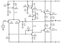
I have a question about the voltage amplification stage of an (audio) amplifier. I just took this attached schematic as an example. The VAS transistor Q4 is driven by the output current from the input pair. It is said the VAS (Voltage Amplification Stage) is a transimpedance stage, converting a current input into a voltage output. But where does this output voltage originates? For example, in the case of a simple common emitter amplifier with a load resistor in the collector path the collector current is converted to a voltage by this load resistor. That's easy to see. But how does this work in the attached schematic, where the load is a current source combined with the output load buffered by the emitter followers.

Where in this schematic is the voltage "created" to provide the output voltage swing to drive the load? Thanks !


Take Q1 input I is , say 2 micro amps, so 200 micro amps flow in collector circuit, across 500 ohms(1k and i/p of Q4) gives about Vo of 100mV for 2 X 10^-6 X 3K = 1.5mV in. I would call it a voltage amplifier.
Q4 is operating into a constant current generator, so its load is mainly the input impedance of two darlington pairs in parallel for small signals where the output transistors are in class A.
Frank
 
Do you know that R2 and R3 are negative feedback and reduce the voltage gain of the entire amplifier to 20?
 
@ Audioguru: Yes i was aware of that, but probably you asked this for a reason :)

@ chuckey: I didn't fully understand your answer.
Take Q1 input I is , say 2 micro amps, so 200 micro amps flow in collector circuit, across 500 ohms(1k and i/p of Q4) gives about Vo of 100mV for 2 X 10^-6 X 3K = 1.5mV in. I would call it a voltage amplifier.

Where does this 3K value come from, I can't see that in the schematic.

Q4 is operating into a constant current generator, so its load is mainly the input impedance of two Darlington pairs in parallel for small signals where the output transistors are in class A.

OK, so the collector load is mainly determined by the input impedance of the Darlington pairs. Then it is the current through this collector load that sets the collector voltage?

If so, then how would we calculate,for example, the quiescent collector output voltage of the VAS transistor?
 

3K is the input impedance of Q4. Yes. If the output is not zero volts current flows down R3, so Q2 adds/reduces the current current in Q1, which changes the output voltage back to zero. Its called negative feedback. For maximum DC stability, R2 should have a capacitor in series with, so the feedback at DC is 100%, and the AC gain would be the same. The capacitor would need a high value resistor across it (100K?) so Q2's bias current has some where to come from.
Frank
 

Isn't the input impedance of Q4: (beta + 1)*R6 ? The datasheet of Q4 (2N5551) lists a beta between 80 and 250. With R6 being 22 Ohm then max. input impedance would be 5.5 kOhm and min. 1.7kOhm. I assume you took an arbitrary value for beta?

Just for a calculation example: If we would have an 8 Ohm load and a beta of 100 for the driver transistors and 50 for the output transistors, so overall beta is 50 *100 = 5000, then the collector would see a load of 5000 * 8 Ohm = 40000 Ohm. Then the current through this 40000 Ohm load is what sets the collector voltage? Then the collector voltage is calculated by +35V - (Ic * 40000 Ohm)? Is this correct?
 

Hi, I'm still struggling with some things in the attached amplifier circuit:

1. How can we find the quiescent bias collector voltage of the VAS transistor (Q4) of this circuit?

2. With the "bias spreader" we create a voltage of 4*Vbe to bias the driver and output stage. How do we make sure this voltage is centered around ground (so the top node of bias spreader is at +2Vbe and bottom node at -2Vbe) for quiescent conditions?
 

The output voltage will be centered at 0V automatically by design of the feedback circuit.
 
If you section the design into 3 stages;


  • 1st stage is a differential input current amplifier with Vgain controlled by R2/R1 ratio =1
    [*=1]and serves to raise input impedance
    [*=1]and control loop V gain from R3, R1 divider ratio.
  • 2nd stage is a single input differential output voltage amp.
    [*=1]with high V gain controlled by CC on both complementary current sharing collectors.
  • final stages are a high current gain (hfe²), Darlington amplifiers which feedback voltage to R3 R1 divider ratio

Thus all the V gain is in the middle stage which must only be >> 20 to remain true with negative feedback.
The approximate gain is the ratio of collector/emitter impedances or (R8+R8)/R6 ~ 1718/22= 78 which satisfies >>20.
 
I see how the negative feedback sets the bias point now. Then how can we determine the quiescent collector current through Q4? As i see it there are actually two opposing current sources. One is a current sink (Q4 itself) and the other is the current source (Q6 and Q7). So which of them sets the current?
 

The quiescent current is forced by Q7 as its a constant current generator. This also gives it a high output impedance so the stage gain of Q4 is greater then R+R7/R6 more like 10K/22 ~ 500. The action of Q5 is to drop the 4 times Vbe at the 10mA supplied by Q7. The resistors around it were selected to give a standing current through the output transistors (10 - 60mA normally).
Frank
 
Last edited:
The current in Q4 is set by the constant current source made with Q6 and Q7. Since the current source has a high impedance then the gain of Q4 is high but its distortion is low.
 
I can see that the current source (Q6 and Q7) wants to provide 10mA through the circuit. But this current also depends on Q4 itself right? Q4 itself functions as a variable current sink set by its base voltage. So the amount of current Q4 let's through its collector depends on its base voltage?
 

If Q4 is shorted then the current from the constant current source is 10mA. If Q4 is almost turned off so that the constant current source still has a few volts to work then its collector voltage is high but its current from the constant current source is still almost 10mA. Q4 tries to change its output current but it cannot. It changes its output voltage instead. Of course its voltage gain is not infinity because some of the current from the constant current source goes to its load then the current through Q4 is affected by its load.
 

Q4 is Q pt is determined by solely due to low impedance thru Vbe of both Q9,Q11 which is defined solely due to the fact that when Vin=0 and R2 reference is GND , the output MUST be zero.
Since R17 is 517 Ω, Vbe will be 517 mV minimum voltage with bias current is my guess.

The 10mA stage 2 bias current is determined by Q6-Ic and Rbe=62Ohms. If Q4-Ic is 10mA then Q6-Ic will be a maximum of 10% of this or 1mA and then Q6-Ib will be a maximum of 10% of Ic which is 100uA which generates 620 mV across Vbe and thus Ic= 630mV /62R= 10 mA.


So what is the output stage bias current? I can see the value of R7/R8 ratio controls it , now how to explain it?

When any normal transistor saturates fully we expect the spec lists a current gain of 10 or Ic/Ib=10.

All datasheets confirm this in the tables and the VI curves for moderate currents around 5A.

We know the output stage can drive AT LEAST 10mA*10*10= 1A when saturated and much more when not saturated.
Now looking closer at the VI curves... calculate the incremental slope of ΔV/ΔI near saturation. Diodes Inc calls it Rce [mΩ] on their patented devices, others call it incremental saturation resistance. I prefer to call this.. ESR for collector saturation . Both NPN-PNP final stage can supply 5A at Vce=5V with hFE=35 but this drops sharply at 10A then hFE drops to 10 at 20A. but at 5V/5A @25'C, the ESR appears to be in Fig 7&8 for ΔIc=20A , ΔVce=1V, thus ESR= 50 mΩ so adding 330 mΩ after each emitter stabilizes the voltage bias between the collectors of stage 2 to protects he final stage in from minor Vbe variations which can lead to "thermal runaway" where bias increases current and Vbe drops and I bias increases. Vce rises out out saturation current gain increases and Pd melts the solder joints. ;)

So what is the voltage of 2nd stage high side collector? Well its defined by the Vbe drops of 2 cascaded complementary Darlingtons. If Vbe-0.5V the Collector to Collector V drop is 2V and at this point we want Vbe on Q5 to also be 0.5V thus with 10mA and 518 Ω we get 518mA as the designer's choice for minimal output bias current , which you may calcuate in your leisure.


This is ok for small input signals but it the input is large such that the 2nd stage will try to saturate.
With Vin=0 the voltage drop across R8(1200 Ω)+R7(512 Ω) with 10mA is 1712 Ω*0.01 A= 17.1V shared by both complementary collectors. So it was designed for 35V dual supplies for large signal output.

But wait a minute, if Q5 starts to turn off and the stage 2 differential voltage across R7+R8 with 10 mA would rise to was 17V with 1.2k+518 Ω gives 1.7kx10mA= 17V !!

So we see when the output stage becomes starved for bias current the voltage gain of stage 2 rises to 78 with 17V across Q5-Vce and this is when all the 10mA goes into the Darlington stages and the device has maximum hfe with Vce far away from saturation.

In general this is a a low voltage gain Class A-B power amp but when the output stage becomes starved for current due to any condition such as a motor or woofer back EMF, the voltage gain rises to increase bias current to maintain excellent load regulation of the voltage, adequate gain for a nominal gain of 20. But we can see that the voltage swing can change the lower the gain dynamically. The minimum gain depends solely on the impedance of Q5 which is dynamically control by output stage bias current . I would estimate Q5_Rb as 359Ω and its collector emitter impedance divided by saturated current gain of 10 so this value divided by emitter R gives the stage 2 minimum gain of approx. 36 Ω /22 Ω = 1.6 so the dynamic voltage gain is reasonably effective at keeping Ie on the output stage slightly higher than the load current.

.... Making it a very efficient and stable Class A-B potential 250W+ RMS power Amp. with suitable thermal design. with only +/-35V supply.
 
Last edited:

Status
Not open for further replies.

Similar threads

Part and Inventory Search

Welcome to EDABoard.com

Sponsor

Back
Top