Continue to Site

Welcome to EDAboard.com

Welcome to our site! EDAboard.com is an international Electronics Discussion Forum focused on EDA software, circuits, schematics, books, theory, papers, asic, pld, 8051, DSP, Network, RF, Analog Design, PCB, Service Manuals... and a whole lot more! To participate you need to register. Registration is free. Click here to register now.

[SOLVED] Output voltage of 555 timer (compatible with other IC's?)

Status
Not open for further replies.

tahir4awan

Full Member level 4
Joined
Nov 29, 2010
Messages
208
Helped
16
Reputation
32
Reaction score
17
Trophy points
1,308
Location
Germany
Activity points
3,084
Hallo,

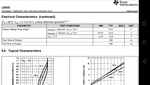
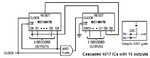
I am building a project on Proteus. It is a LED chaser with 555 and 4017. The Problem is, in Simulator voltages are totally different. For example if I check output voltage of 555, it says 5V. But I have read Datasheet in which Output voltage is 3.3V. If I connect Output of 555 to Input CLK Pin of 4017 in Simulator it will Work fine. But If I use Manual Signal of 3.3v to Input CLK pinof 4017 in Simulator it will not Work.

I have searched, but could not able to find, that how much voltage and current need for an Input CLK of digital ICs.

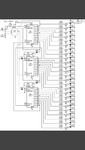
Secondly can I connect Output Signal of 4017 directly to a Flip Flop. Because in Simulator Output voltage is again 5V. But I am not sure about current ranges. Do I need Transistors to ampilfy current?


Thanks
--- Updated ---

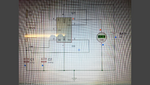
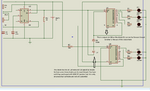
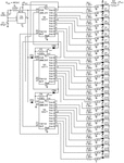
This is the Project. Instead of Leds output from 4017, I want to use Latch Flip Flops and then Leds.
 

Attachments

  • 3euh3.gif
    3euh3.gif
    19.3 KB · Views: 883
Last edited:

The schematic is wrong!

The 'OUT9' signals should be the only thing feeding the 'CLK' on the CD4017s. What you are seeiing is the clock voltage being pulled low from the previous stage through the diode. Check the data sheet for how to cascade CD4017 devices.

Brian.
 

    tahir4awan

    Points: 2
    Helpful Answer Positive Rating
Hi,

When you refer to datasheets, please post a link.
When you refer to a proteus simulation, then show your proteus file.
With the given infirmations we are not able to validate the circuit and values.
When you compare voltages between datasheet and simulation, be sure you have the identical test conditions.
In the datasheet they should be given.

You say CD4017 works with 5V input voltage. If I'm not mistaken CMOS input High level should be at least 0.7 x VCC. At 9V VCC this means 6.3V.
3.3V won't be sufficient. With 5V it may work, but there is no guarantee. Keep on the datasheet to get reliable operation.

You say you don't find CLK input current and voltage. I wonder...please post the (link to) your datasheet.
Usual abbreviations are VIH, VIL, Iin...or so...
Input currents of CMOS ICs usually are negligible.

I doubt the wiring is correct. But did not go deeply through it.

Klaus
 

    tahir4awan

    Points: 2
    Helpful Answer Positive Rating
This is the Screenshot of 555. As you can see supply voltage is 5v and Output is also 5v and not 3.3v mentioned in Datasheet.
--- Updated ---

Datasheet
--- Updated ---

Its working.
 

Attachments

  • Screenshot_20201122-185720.png
    Screenshot_20201122-185720.png
    3.3 MB · Views: 285
  • Screenshot_20201122-185026.png
    Screenshot_20201122-185026.png
    328.1 KB · Views: 261
  • Screenshot_20201122-190923.png
    Screenshot_20201122-190923.png
    3 MB · Views: 190
Last edited:

Hi,

You did not take 10Mbyte photos (of bad quality) of your monitor instead of using "screenshot" functionality...(with perfect results)?

Your 555 is supplied with 5V... and on another schematic it is supplied with 9V.
An unloaded output may go high to VCC because of leakage currents. Thus it makes sense to load the output to get more reliable results.
And the datsheet gives "min" and "typ" value. "Max" is not given. Thus 5V is within specification.

Klaus
 

    tahir4awan

    Points: 2
    Helpful Answer Positive Rating
Thank you very much Klaus for your precious help. I really appreciate that. And Brayan thanks for your correction.
 

I want to use Latch Flip Flops and then Leds.

This doesn't go as far as handing you the solution but it demonstrates the strategy of multiplexing using a flip-flop.

One 4017 IC can sequence 20 led's. A toggle flip-flop provides a path to ground for one row of led's at a time. Outputs Q and Q-bar switch states back and forth to two rows of led's.

4017 IC sequencing 20 led's one at a time via toggle flip-flop.png


With the addition of more logic gates you can expand this to 3 or 4 stage multiplexing. It's your decision whether you choose instead to add another 4017 IC, depending on the degree of complexity of the circuit.
 
  • Like
Reactions: d123

    tahir4awan

    Points: 2
    Helpful Answer Positive Rating

    d123

    Points: 2
    Helpful Answer Positive Rating
Amazing! Yes your right with more 4017 it i'll get more complicated.
 

Hi,
With the addition of more logic gates you can expand this to 3 or 4 stage multiplexing.
Good idea.
What about using another shift register for "row" selection? --> Up to 100 LEDs
But not multiple LEDs ON at the same time.

Klaus
 
Did someone else notice Problem with this schematic as Brian mentioned. I find it also Strange. Two Diodes in Reverse biased Mode. But strangely its working in Simulator.
 

Attachments

  • Screenshot_20201120-220934.png
    Screenshot_20201120-220934.png
    329.1 KB · Views: 179

Hi,

two diodes = wired_AND
I guess the diodes "disable" the clock. Usually thats what the INHIBIT input is for.

Klaus
 

What I am not able to understand, how these Diodes get Forward biased. The clock voltage is 5v the Vcc is also 5v. For uper 4017 it is cleared but for lower 4017 it is getting clock Signal from Vcc. When Q9 Pin of lower 4017 is active it will disable the uper 4017 but how come the current get throug Diodes for lower 4017 CLK Signal. I dit it separatley in Simulator the clock voltage for both ICs were almost Same but there was huge differnce in current. CLK 1 war 5mA and clock 2 war 700 nA. So both CLK are mit getting the Same amount of current. Which is confusing.
 

The diodes are never reverse biased. The anode connects to the 100k resistor that is connected to the positive supply. When the cathode is high then the diodes do nothing but when the cathode is low then the diode conducts and makes its anode low.
Look at the 3rd CD4017 U4, its Inhibit pin13 is grounded so that it always counts.

EDIT: A CD4017 is Cmos. A Cmos IC CLOCK pin or any other input draws NO current.
 

Some functional simulation models for the 555 do not generate the proper high output of a real bipolar 555 (which is around 1.5V below the plus supply voltage).
For a real 5V output from a 5V supply, you can use the CMOS version of the 555 (e.g. LMC555), but note its output current drive capability is less.
 

The diodes are never reverse biased. The anode connects to the 100k resistor that is connected to the positive supply. When the cathode is high then the diodes do nothing but when the cathode is low then the diode conducts and makes its anode low.
Look at the 3rd CD4017 U4, its Inhibit pin13 is grounded so that it always counts.

EDIT: A CD4017 is Cmos. A Cmos IC CLOCK pin or any other input draws NO current.

Here what I understood from schematic.
 

Attachments

  • Unbenannt.png
    Unbenannt.png
    20.2 KB · Views: 153

The 2 diodes and R7 are an AND gate. Both cathodes must be high for their combined anodes to be high which is the clock trigger for U2.
Like here:
 

Attachments

  • cascaded 4017s-3.PNG
    cascaded 4017s-3.PNG
    14.3 KB · Views: 159

    tahir4awan

    Points: 2
    Helpful Answer Positive Rating
Status
Not open for further replies.

Part and Inventory Search

Welcome to EDABoard.com

Sponsor

Back
Top