farhan89
Junior Member level 3
Hello,
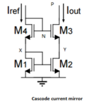
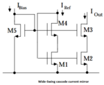
I have a small confusion regarding the Output resisitance of Cacode current mirror and Wide wing cascode current mirror. As per my knowledge, both of these have same output resistance. But when I calculated thru AC simulation its giving me different values for resistance.

Kindly see the attached images. Both configuration have identical transistors. M4=M1 and M2=M3, M2 and M3 has twice width of M1 and M4 and M5 gate length is 4 times of other transistors. IREF is 50 uA and V_OUT is 1.2 V, Ibias is 200uA, in DC simulation I can measure the I_OUT (100uA) , for AC simulation I am inserting 1 V AC at output and measuring the current at output (R=V/A). In Cascode it is around 569K ohm and in Wide swing it is 600 Kohm.
Could anyone explain me why is this so ? If I decrease the Ibias (in wide swing) then resistance is decreasing.
Any hints
I have a small confusion regarding the Output resisitance of Cacode current mirror and Wide wing cascode current mirror. As per my knowledge, both of these have same output resistance. But when I calculated thru AC simulation its giving me different values for resistance.


Kindly see the attached images. Both configuration have identical transistors. M4=M1 and M2=M3, M2 and M3 has twice width of M1 and M4 and M5 gate length is 4 times of other transistors. IREF is 50 uA and V_OUT is 1.2 V, Ibias is 200uA, in DC simulation I can measure the I_OUT (100uA) , for AC simulation I am inserting 1 V AC at output and measuring the current at output (R=V/A). In Cascode it is around 569K ohm and in Wide swing it is 600 Kohm.
Could anyone explain me why is this so ? If I decrease the Ibias (in wide swing) then resistance is decreasing.
Any hints