Continue to Site

Welcome to EDAboard.com

Welcome to our site! EDAboard.com is an international Electronics Discussion Forum focused on EDA software, circuits, schematics, books, theory, papers, asic, pld, 8051, DSP, Network, RF, Analog Design, PCB, Service Manuals... and a whole lot more! To participate you need to register. Registration is free. Click here to register now.

Output rectifier for One transistor forward SMPS?

Status
Not open for further replies.

cupoftea

Advanced Member level 5
Joined
Jun 13, 2021
Messages
2,589
Helped
54
Reputation
108
Reaction score
115
Trophy points
63
Activity points
13,602
Hi,
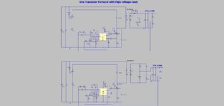
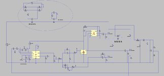
The following are both one tran forwards (LTspice and jpeg) .....with well known output rectifiers.
1.....Well known Direct diode rectifier
2...Well known Capacitively coupled rectifier

Do you agree that the capacively coupled output rectifier is a waste of time?......the peak currents are way higher...OK, the voltage on the output diode is much less...but so what...you can get 900V fast diodes....and 900V sync FETs.
 

Attachments

  • One transistor forward _rectifier comparison.zip
    3.6 KB · Views: 67
  • One tran forward _rectifier compare.jpg
    One tran forward _rectifier compare.jpg
    120.3 KB · Views: 87

Thanks, but capacitive coupled output rectifier is a well known, bona fide scheme.
As you know, the forward core only saturates on iMag..and thats low...just as low as the other one.
 

Expect core saturation with capacitive coupled output.
Thanks, ayk, the capacitive coupling ensures there is no net DC in the secondary, as such, it cannot saturate, may i ask, is this what you meant?
 

Not at all. The forward converter has DC in the primary that has to be compensated by secondary current. Capacitor is blocking compensation option.
 
Thanks, yes, woops, i was forgetting the pri.....though when current flows in the pri, current also flows in the sec, and the mag field of the sec current cancels that of the pri.....AYK, that still applies even when the series capacitors are used. As such, using series-capacitor-rectifier wont worsen the situation pertaining to saturation?...compared to the "normal" non series capacitor rectifier?
 
Last edited:

Consider that integral(n1*i1) must balanced with integral(n2*i2). Abstracting from small primary reset current integral, this can be only achieved with DC coupled secondary, a capacitor enforces integral(n2*i2) = 0.
 
I don't think either will work well because both lack an output choke, which is required for a forward converter to operate properly.
Thanks, but capacitive coupled output rectifier is a well known, bona fide scheme.
[citation needed]
 
I don't think either will work well because both lack an output choke, which is required for a forward converter to operate properly.
Thanks, i have it on my bench now, its working excellently, running very cool (i dont have schem, BOM or layout).....its doing 150W from 90-265vac, and passing mains harmonics class A...and uses just a PQ26/25.....Total primary capacitance is 33uF,500v,'lytic and a 5u6, 450V, film.
Its using the time old , well known technique of shovelling the leakage and magnetising inductance energy into the 33uF. The 33uF is only drawn from in the hi-side fet cycle.

Consider that integral(n1*i1) must balanced with integral(n2*i2). Abstracting from small primary reset current integral, this can be only achieved with DC coupled secondary, a capacitor enforces integral(n2*i2) = 0.
Thanks, though , AYK, gate drive transformers use capacitive coupled secondary.

Also, the problem is, when you just have a burden resistor across the secondary, how can the current sense transformer ever get reset?....hence a series capacitor is also needed. The sim shows it working in LTspice as attached. If the sim is wrong, then you have to ask, what law of physics has the simulator (LTspice) broken?
"n2i2 = n1i1" is preserved.
"v.s (ON) = v.s (OFF)" is preserved

Yes the sec current is displaced, but thats the price i am willing to pay for a CST that can measure primary current that is either unidirectional, balanced-bidirectional, or non-balanced-bidirectional.

....I take it that you are implying that the small net voltage across the primary will eventually saturate the CST?
 

Attachments

  • CST in 2 tran forward.jpg
    CST in 2 tran forward.jpg
    167.2 KB · Views: 63
  • Two tran forward_CST.zip
    3 KB · Views: 56
Last edited:

FvM is correct. In your own simulation, the top circuit maintains net flux in the transformer near zero, while the bottom circuit has a large DC offset. Did you even bother to check?

1679658551830.png
 

Surely the 3 caps on the output form a short term short ckt every time the main mosfet turns on - resulting in a turn on current spike and extra turn on losses ?
 
Surely the 3 caps on the output form a short term short ckt every time the main mosfet turns on - resulting in a turn on current spike and extra turn on losses ?
Thanks but no i dont see any such current spike either in the sim or the SMPS that i have on the bench...i have copiously probed its every power branch with CSTs...no current spikes.
There is a large leakage inductance in the transformer.

BTW, the primary side that i show is not strictly what i have here on the bench...i am not allowed to show it...it is our suppliers IP....they want us to buy it, but wont show us any schem etc until we front up the dosh.
Its kind of like a forward/Half bridge....there is asymetric switching, there is a 33uF pri side cap which gets used for power throughput at bottom of half sine....AYK, because its not flyback it needs this.

What i have on the bench, i would call kind of..an "asymetric half bridge."...ish......the totem pole of two FETs switch like a synch buck does it.

FvM is correct. In your own simulation, the top circuit maintains net flux in the transformer near zero, while the bottom circuit has a large DC offset. Did you even bother to check?
Thanks, AYK, Acive clamp forwards often have such a dc offset, when they use significant leakage inductance...and the leakage inductance kind of provides safety in this situation of "otherwise peril".

As discussed, what i have here as i said, is not exactly what i show in this post.....kind of i am thinking you will work out what i have on the bench in front of me....i am not allowed to show it. But yes, the algorithm should measure the Voltages and make v.us equal for ON and for OFF.......then, in this particular converter....the frequency is adjusted to vary the power throughput....
BTW, the secondary of what i show is exactly what i have on the bench here.

Also, due to the high leakage inductance, its not possible to assess the turns ratio from the normal N1.I1 = N2.I2 or vp/vs = np/ns.

The turns ratio measures as 8:1, (using LCR6200) which appears to show that for much of the time, it relies on the charged up 33uF, 500V capacitor to get power throughput.

The long and short of it is that this is a single stage PFCd converter of 150W, using just a PQ26/25, and the 33uF , 500V lytic capacitor, and a 5u6 450v film cap, ....and the "glory statement" is that this is the smallest earthly way to get 150W single stage PFC. (100-265VAC IN, 37VOUT, 150WOUT).
So i am working out if this is true or not.
--- Updated ---

So, yes, that top diode is actually a fet in the pri side...but i cant show that......i dont really see the potential in this, and am just working through it to provide the proof, so to speak.
I mean, 150W single stage PFC from 100-265vac, and PQ26/25 + 33uF, 500V + 5u6.450V......doesnt seem any better than a BCM flyback PFC...but i have to work through it and proove it.
 
Last edited:

Status
Not open for further replies.

Similar threads

Part and Inventory Search

Welcome to EDABoard.com

Sponsor

Back
Top