Continue to Site

Welcome to EDAboard.com

Welcome to our site! EDAboard.com is an international Electronics Discussion Forum focused on EDA software, circuits, schematics, books, theory, papers, asic, pld, 8051, DSP, Network, RF, Analog Design, PCB, Service Manuals... and a whole lot more! To participate you need to register. Registration is free. Click here to register now.

[SOLVED] Output Power Pull down on custom 6GHz PCB design

Status
Not open for further replies.

Nalqahtani

Newbie
Joined
Feb 7, 2021
Messages
5
Helped
0
Reputation
0
Reaction score
0
Trophy points
1
Activity points
67
I have designed a 6GHz PCB, containing the HMC358 VCO, PMA3-83LNW+ LNA and several other components.

Testing the VCO output using an UHF reads 11dBm, which is excellent. However, this is the input to an LNA on the same board, once this LNA is soldered on the board, the VCO's output at the UHF reads 0.5dBm (drops significantly). I would like to know the reason behind this and how to prevent this from happening.

Further details are listed below
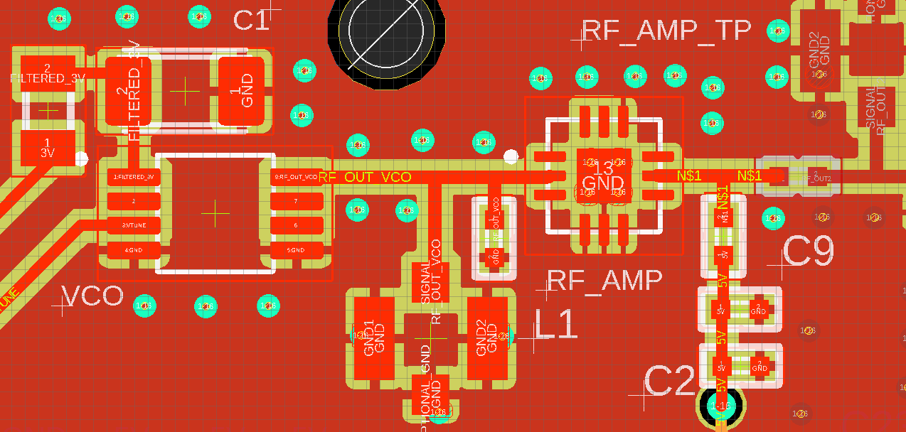
top layer.PNG


The image shows a VCO on the left, followed by a test point, which showed 11dBm at first. Once soldering the LNA with its required components, the power measured at the VCO test point dropped to 0.5dBm. The amplification of the LNA is 20dBm at 6GHz. However, the measured output at the LNA test point was 11 to 12 dBm.
I'm wondering why this significant pull down. Is it the FR4 board? Is it the ground pour surrounding the traces? Is there a mismatch due to the trace width? Or is it the pads and the trace transition needs to be smoother.

I have been redesigning this quite some times to tackle the power loss. I'm not seeing the light at the end of the tunnel, it only keeps getting darker and darker.
Any help is highly appreciated!

Its built on a 4 Layer FR4 board purchased from JLC PCB. It was an impedance controlled fabricated in JLCPCB, using their JLC7628 stack-up (https://cart.jlcpcb.com/impedance?_ga=2.109258054.2129155813.1617134999-848782461.1614671184)

The VCO datasheet is
https://www.analog.com/media/en/technical-documentation/data-sheets/hmc358.pdf

The LNA datasheet is
https://www.minicircuits.com/pdfs/PMA3-83LNW+.pdf

The trace width calculated to operate at 6GHz on the FR4 (diel. con. =4.6) was 0.349 mm
Top layer is GND, RF and analog traces (kept away from the RF)
2nd Layer is GND
3rd Layer is Power (5v and 3v)
4th Layer is GND

Thank you :)
 

The image shows a VCO on the left, followed by a test point, which showed 11dBm at first. Once soldering the LNA with its required components, the power measured at the VCO test point dropped to 0.5dBm.

Do you test this with both 50 Ohm load at the test point AND the amplifier IN PARALLEL?

This is not possible, you need to switch between one of the loads at at time. Coax out OR amplifier, but not both in parallel.
 
Because your PCB layout is too bad for 6GHz..
in ALL aspects..
-A Connector cannot be tapped to a Miscrostrip Line
-Thermal Reliefs ( GND Connections) are very bad idea for Rf and Microwave Frequencies
-Copper Pour all around the components is too bad idea for 6GHz ( it's acceptable perhaps 100 MHz) due to unwanted capacitive couplings.
VCO must be grounded by its ground plate with many vias..
etc. etc..
-You got a long way to run..
 

Do you test this with both 50 Ohm load at the test point AND the amplifier IN PARALLEL?

This is not possible, you need to switch between one of the loads at at time. Coax out OR amplifier, but not both in parallel.

Thank you for your response. I would test them separately and not at the same time (parallel)

The way I was testing the component is, I would solder the VCO first, test it and check the power out. The datasheet mentioned a maximum output power of 11dBm, which was achieved at that test point.

I would then solder the LNA and test the LNA from the LNA test point only it would be still 11 to 12 dBm. I would disconnect the UHF test point from the LNA test point and connect it to the VCO to check the VCO output, then I would notice it drops from its first measured 11 dBm to about 0.5 dBm.

Thank you
 

Because your PCB layout is too bad for 6GHz..
in ALL aspects..
-A Connector cannot be tapped to a Miscrostrip Line
-Thermal Reliefs ( GND Connections) are very bad idea for Rf and Microwave Frequencies
-Copper Pour all around the components is too bad idea for 6GHz ( it's acceptable perhaps 100 MHz) due to unwanted capacitive couplings.
VCO must be grounded by its ground plate with many vias..
etc. etc..
-You got a long way to run..

Thanks for your response.

I appreciate your recommendations, the ones you mentioned will help refine the design.
The UHF connectors were placed in order to be able to test each RF component separately in a cost effective way. I was not aware it shouldn't be done

Do you have any further recommendations? Can you point me towards a documentation that discusses PCB layouts for 6GHz?

I know I've got a long way to go, but it's all a learning process in the end and I'm here to learn. Whether its from professionals like yourself or from others.

Thanks
 

I would then solder the LNA and test the LNA from the LNA test point only it would be still 11 to 12 dBm. I would disconnect the UHF test point from the LNA test point and connect it to the VCO to check the VCO output, then I would notice it drops from its first measured 11 dBm to about 0.5 dBm.

Sorry, I don't understand your test description.

In any case, 11dBm at the input of your LNA is too much. Look at the LNA data sheet, it has 22dB Gain and can deliver 22dBm output power. That would be around 0dBm input power.

Do you have good ground at the LNA ground paddle? I don't see vias there.

Having the unconnected coax as an open ended stub connected to the trough line is not correct RF design, it will create a reactive load to the line. Usually we have 0 Ohm jumpers which route RF to one of the two paths, so that we can switch to the coax by soldering the 0 Ohm bridge from one path to the other.
 

    Nalqahtani

    Points: 2
    Helpful Answer Positive Rating
I'm sorry if my description did not make much sense. I'm new to RF design (obviously) and I thought this UHF connectors after each major RF component would be handy way to investigate the output power.

The LNA has 4 vias connecting the LNA's ground pad to the ground plane. They're difficult to spot in the image.

The 0 Ohm Bridge resistor is a brilliant idea, thank you for that. So in this case, I could use 2x 0 Ohm resistors, one prior to the UHF stub and one for the through line. I would only solder the first to use the UHF port to test the LNA. Once tested, desolder the first 0 ohm resistor for the UHF and solder the 2nd 0 ohm resistor for the through line. That's brilliant sir!

Thanks a million for this.

Do you have any other insights that may help ?
 

As was mentioned, your PCB layout is way far to be acceptable at 6GHz. This is your first step that have to solve.
Because today mmWave frequencies above 30GHz became very common in industry, people think that 6GHz is a "piece of cake" domain, and is as easy to deal as audio frequencies.
 

As was mentioned, your PCB layout is way far to be acceptable at 6GHz. This is your first step that have to solve.
Because today mmWave frequencies above 30GHz became very common in industry, people think that 6GHz is a "piece of cake" domain, and is as easy to deal as audio frequencies.

Vfone, I appreciate your comment. However, your comment doesn't really provide any helpful insight or useful feedback. The other members actually pointed me towards solutions that would help.

Maybe share why you think its far from acceptable, so I can actually learn and take that first step in solving my issues.
 

Status
Not open for further replies.

Part and Inventory Search

Welcome to EDABoard.com

Sponsor

Back
Top