Continue to Site

Welcome to EDAboard.com

Welcome to our site! EDAboard.com is an international Electronics Discussion Forum focused on EDA software, circuits, schematics, books, theory, papers, asic, pld, 8051, DSP, Network, RF, Analog Design, PCB, Service Manuals... and a whole lot more! To participate you need to register. Registration is free. Click here to register now.

Output port is completely "don't care"

Status
Not open for further replies.

mohamis288

Full Member level 3
Joined
Mar 1, 2022
Messages
164
Helped
0
Reputation
0
Reaction score
1
Trophy points
18
Activity points
1,235
Hello,

I have simulated the 8-bit FIR filter in Questa, But as you can see some ports are in 'don't care' status. I am new to the digital design. so I need your help.
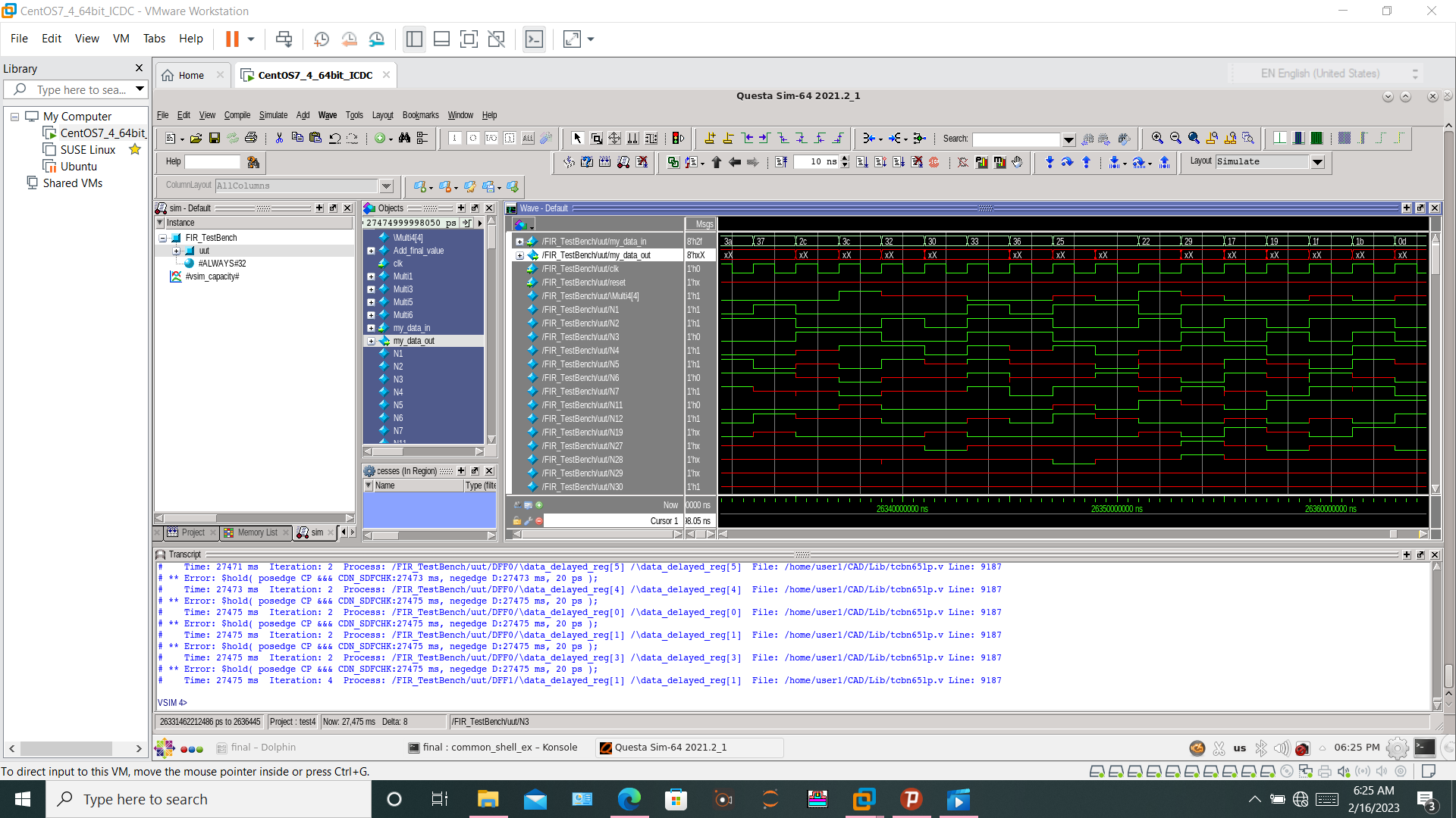
1676557541214.png


I have used design vision to synthesize my Verilog code. But I did not define the clock period, input delay, output delay and ...

is this problem related to that? how can I solve it?

BR
 

Actually, 'X' means that the value is forcing unknown. You may need to show your codes.
 

It's probably an initialization problem. As kazi says, assert your reset and see if that solves your problem. If not, then there's something in your design that is not properly initializing one or more signals.
 

At least the reset signal should be driven.
@barry
@Akanimo

you are right. my reset does not work. I changed the value of reset between 0 and 1 but output is 'don't care' yet. actually, there is some error messages in the transcript like this:

Code:
** Error: $hold( posedge CP &&& CDN_SDFCHK:29215 us, negedge D:29215 us, 20 ps );
#    Time: 29215 us  Iteration: 10  Process: /FIR_TestBench/uut/DFF4/\data_delayed_reg[4] /\data_delayed_reg[4]  File: /home/user1/CAD/Lib/tcbn65lp.v Line: 9187

I think the problem is related to this. I modify my question with my Verilog code. if you have any suggestion, let me know. thank you.

--- Updated ---

question modifications


original code:
Code:
`timescale 1ns / 1ps

// Module Name: FIR_Filter


module FIR_Filter(clk, reset, my_data_in, my_data_out);

parameter N = 8;

input clk, reset;
input [N-1:0] my_data_in;
output reg [N-1:0] my_data_out;

// coefficients defination
// Moving Average Filter, 3rd order

wire [7:0] b0 =  8'b00001010;
wire [7:0] b1 =  8'b00010000;
wire [7:0] b2 =  8'b00101000;
wire [7:0] b3 =  8'b01000000;
wire [7:0] b4 =  8'b00101000;
wire [7:0] b5 =  8'b00010000;
wire [7:0] b6 =  8'b00001010;


wire [N-1:0] x1, x2, x3, x4, x5, x6;

// Create delays i.e x[n-1], x[n-2], .. x[n-N]
// Instantiate D Flip Flops
DFF DFF0(clk, 1'b0, my_data_in, x1); // x[n-1]
DFF DFF1(clk, 1'b0, x1, x2);      // x[x[n-2]]
DFF DFF2(clk, 1'b0, x2, x3);      // x[n-3]
DFF DFF3(clk, 1'b0, x3, x4);     
DFF DFF4(clk, 1'b0, x4, x5);
DFF DFF5(clk, 1'b0, x5, x6);


//  Multitiplication
wire [N-1:0] Multi0, Multi1, Multi2, Multi3, Multi4, Multi5, Multi6; 
assign Multi0 = my_data_in * b0;
assign Multi1 = x1 * b1; 
assign Multi2 = x2 * b2; 
assign Multi3 = x3 * b3; 
assign Multi4 = x4 * b4; 
assign Multi5 = x5 * b5; 
assign Multi6 = x6 * b6; 

 
// Addition operation
wire [N-1:0] Add_final_value;
assign Add_final_value = Multi0 + Multi1 + Multi2 + Multi3 + Multi4 + Multi5 + Multi6;

// Final calculation to output
always@(posedge clk)
my_data_out <= Add_final_value;

endmodule


module DFF(clk, reset, my_data_in, data_delayed);
parameter N = 8;
input clk, reset;
input [N-1:0] my_data_in;
output reg [N-1:0] data_delayed;

always@(posedge clk, posedge reset)
begin
    if (reset)
    data_delayed <= 0;
    else
    data_delayed <= my_data_in;
    
end

endmodule


test bench:

Code:
`timescale 1us / 1ps
//////////////////////////////////////////////////////////////////////////////////

// Module Name: FIR_TB


module FIR_TestBench;

parameter N = 8;

reg clk, reset;
reg [N-1:0] my_data_in;
wire [N-1:0] my_data_out;

FIR_Filter uut(.clk(clk), .reset(reset), .my_data_in(my_data_in), .my_data_out(my_data_out));

initial
reset = 1;


always
#5 reset = ~ reset;

// input sine wave data
initial
$readmemb("/home/user1/CAD/final/final/signal.tv", RAMM);

// Create the RAM
reg [N-1:0] RAMM [31:0];

// create a clock
initial
clk = 0;
reg [4:0] Address_me;

always
#1 clk = ~ clk; 

// Read RAMM data and give to design
always@(posedge clk)
    my_data_in <= RAMM[Address_me];
    
// Address_me counter

initial
Address_me = 1;
always@(posedge clk)
begin
    if (Address_me == 31)
        Address_me = 0;
    else
        Address_me = Address_me + 1;
end     

endmodule
 

Is your simulation timing or functional?
if timing your clock is 1GH in testbench???
Moreover you better de-assert reset correctly instead of toggling it.


Status
Not open for further replies.

Part and Inventory Search

Welcome to EDABoard.com

Sponsor

Back
Top