Georgiy_Klimov_
Newbie
Hello, dear collegues! I'm currently designing H-bridge converter for DC-motor drive.
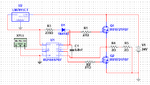
I decided to use bootstrap driver for driving converter MOSFETs. IRF8721PBF were choosen as switches, IR2184 was chosen as a gate driver.
To quickly test their performance I soldered bread board with Half-bridge converter. You can see the circuitry on the figure. There is also decoupling capacitors on inputs of L7815(0,33uF ceramic) and IR2184(0,1uF ceramic).

The problem is the gate voltage drop on upper switch during switching on or it better to say oscilation on upper switch gate.
The oscillograms was pictured and you can see voltages on load, on upper and lower gates, and on Vboot and Vcc pins of IR2184.


I have tried different valiues of Cboot from 6.8nF to 1uF but there is no significant difference between results.
It would be great to get any suggestions concerning the problem.
Thanks
P.S.
I calculated Cboot according to equation from Design Tips "Using monolithic high voltage gate drivers" from Infeneon site.
Cboot=Qtot/dVbs=6.3nF;
Qtot=Qg+Qls+(Ilk_gs+Iqbs+Ilk+Ilk_diode+Ilk_cap+Ids)*Thon=26nC
dVbs=Vcc-Vf-Vgs_min-Vds=4.14V
Bootstrap diode was also choosen accoding to the DT mntioned below so that diode breakdown voltage was lower that DC bus voltage and it had low reverse recovery time (<100ns)
Bootstrap resistor was choosen basing on bootstrap circuit time constant Tboot. Tboot should be five times lower than the minimum time, when lower switch is on.
5*Tboot<1/f_sw*(1-DC); (f_sw - switching frequency, DC-maximum duty cycle)
Tboot<1/20000*(1-0.8);
Tboot<2us;
Tboot=Rboot*Cboot=>
=>Rboot<2us/6.8nC=295 Ohm plus I decided to add some margin, so I have R=235 Ohm
Qg=12nC; Total gate charge
Iqbs=150uA; % Floating section quiescent current
Ilk=50uA; % Floating section leakage current
Ids=0A; %Desat current
Qls=5nC; % Charge required by the internal level shifters
% level shift charge required per cycle (typically 5 nC for 500 V/600 V MGDs and 20 nC for
%1200 V MGDs)
Qp=4nC; % Сharge absorbed by the level shifter. QP is approximately 4 nC at VR = 50 V and increases to 7 nC as the rail voltage increases to 500 V
Qcmos=30nC; % QCMOS between 5 and 30 nC, depending on MGD.
Vcc=15V;
Vf=0.75V;
Vgs_min=10V;
Vds=0.1V;
I decided to use bootstrap driver for driving converter MOSFETs. IRF8721PBF were choosen as switches, IR2184 was chosen as a gate driver.
To quickly test their performance I soldered bread board with Half-bridge converter. You can see the circuitry on the figure. There is also decoupling capacitors on inputs of L7815(0,33uF ceramic) and IR2184(0,1uF ceramic).
The problem is the gate voltage drop on upper switch during switching on or it better to say oscilation on upper switch gate.
The oscillograms was pictured and you can see voltages on load, on upper and lower gates, and on Vboot and Vcc pins of IR2184.
I have tried different valiues of Cboot from 6.8nF to 1uF but there is no significant difference between results.
It would be great to get any suggestions concerning the problem.
Thanks
P.S.
I calculated Cboot according to equation from Design Tips "Using monolithic high voltage gate drivers" from Infeneon site.
Cboot=Qtot/dVbs=6.3nF;
Qtot=Qg+Qls+(Ilk_gs+Iqbs+Ilk+Ilk_diode+Ilk_cap+Ids)*Thon=26nC
dVbs=Vcc-Vf-Vgs_min-Vds=4.14V
Bootstrap diode was also choosen accoding to the DT mntioned below so that diode breakdown voltage was lower that DC bus voltage and it had low reverse recovery time (<100ns)
Bootstrap resistor was choosen basing on bootstrap circuit time constant Tboot. Tboot should be five times lower than the minimum time, when lower switch is on.
5*Tboot<1/f_sw*(1-DC); (f_sw - switching frequency, DC-maximum duty cycle)
Tboot<1/20000*(1-0.8);
Tboot<2us;
Tboot=Rboot*Cboot=>
=>Rboot<2us/6.8nC=295 Ohm plus I decided to add some margin, so I have R=235 Ohm
Qg=12nC; Total gate charge
Iqbs=150uA; % Floating section quiescent current
Ilk=50uA; % Floating section leakage current
Ids=0A; %Desat current
Qls=5nC; % Charge required by the internal level shifters
% level shift charge required per cycle (typically 5 nC for 500 V/600 V MGDs and 20 nC for
%1200 V MGDs)
Qp=4nC; % Сharge absorbed by the level shifter. QP is approximately 4 nC at VR = 50 V and increases to 7 nC as the rail voltage increases to 500 V
Qcmos=30nC; % QCMOS between 5 and 30 nC, depending on MGD.
Vcc=15V;
Vf=0.75V;
Vgs_min=10V;
Vds=0.1V;