Continue to Site

Welcome to EDAboard.com

Welcome to our site! EDAboard.com is an international Electronics Discussion Forum focused on EDA software, circuits, schematics, books, theory, papers, asic, pld, 8051, DSP, Network, RF, Analog Design, PCB, Service Manuals... and a whole lot more! To participate you need to register. Registration is free. Click here to register now.

ORCAD PCB Designer 17.4 Copper plating inside mounting hole

Status
Not open for further replies.

jimmykk

Full Member level 3
Joined
Oct 2, 2014
Messages
158
Helped
0
Reputation
0
Reaction score
1
Trophy points
1,298
Activity points
2,863
Hi

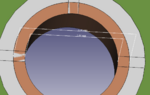
The problem i experience is that the Copper plating inside the mounting holes is shown thicker than it should be. As a result, the actual drill size of hole is not shown correctly. Can't find anything to control Copper thickness in pad file.
example: i made a hole of 3.3mm diameter but in step model there is shown plating copper on hole walls which reduces its diameter to around 2.63mm.
As an observation, Copper plating thickness is set to 20 percent of hole diameter. where can i control it?
 

Hi,

Standard copper thickness us 35um.
In a hole you have two copper platings making a total of 70um copper.
3.00mm - 70um = 2.93mm.

In reality the plated copper in hole walls is thinner.

But usually the board manufacturers care for this. If you say 3.00mm, then it is end-diameter, so they drill slighly wider...3.1mm for example.

The question is: do you want the hole plated at all? (Precision holes usually are not plated)

For details I'd contact the board manufacturer.

Klaus
 

Hi

I know the actual plating thickness is much lower. But the maths does not add up here.
Desired Drill diameter is 3.3mm and what i see after plating as shown below is 2.64mm which is much lower than actual.
It is only the step model which is the issue here.
 

Attachments

  • drill.PNG
    drill.PNG
    42.2 KB · Views: 192

Hi,

I did not read/understand the numbers correctly.
--> my above post makes no sense, then. Sorry.

I've no explanation how your software comes to these values.

Klaus
 

Actual PCB is not a problem as i decide the stackup for manufacturer myself and can change/see plating thickness.
But it is only the 3d viewer which is creating mess here.
 

I would never bother with plating or copper patterns on a step file, unnecessary excess data that you don't need in the 3D world for fit and form.
The only time you may ever need a copper pattern is if some really serious physical simulations are necessary. In the last few years since IDF transfer has been available, I have only done it twice, once for a space borne design and one for some sensors to go on very small birds. Both heavily funded projects.
For creating STEP files leave the copper off, it just makes the files large for no reason.
 

Status
Not open for further replies.

Part and Inventory Search

Welcome to EDABoard.com

Sponsor

Back
Top