Continue to Site

Welcome to EDAboard.com

Welcome to our site! EDAboard.com is an international Electronics Discussion Forum focused on EDA software, circuits, schematics, books, theory, papers, asic, pld, 8051, DSP, Network, RF, Analog Design, PCB, Service Manuals... and a whole lot more! To participate you need to register. Registration is free. Click here to register now.

opamp voltage follower

Status
Not open for further replies.

jayanthyk192

Full Member level 3
Joined
Sep 17, 2010
Messages
179
Helped
1
Reputation
2
Reaction score
1
Trophy points
1,298
Activity points
2,580
Hi,

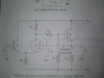
i started learning about opamps from a book by David Bell.I'm stuck up in the voltage follower cirucit(attached).i'm not able to analyze the circuit as there are too many parameters coming in.firstly the voltage V1 is increased,and according to the book the V feedback and hence V2 @ Q2 is zero.i did'nt understand this.then as the votage is increased all parameters sort of come together and makes my analysis difficult.so how do i analyze the circuit. j.jpg
 

It's great that you have a mind for the math aspects of electronics.

A voltage follower gives you more power available to drive the next stage. That's the simple definition.

It isolates the preceding stage from circuitry downstream.

The word follower refers to the idea that its output closely follows the input V.

You're probably referring to the fact that there's a resistor between emitter to ground. This can be used to send a feedback effect to the bias control circuit.

However feedback is not normally acting in this case ... however it would if you were to attach something drastic at the output, and conceivably that would disrupt the inner workings of the op amp.
 

It's great that you have a mind for the math aspects of electronics.

A voltage follower gives you more power available to drive the next stage. That's the simple definition.

It isolates the preceding stage from circuitry downstream.

The word follower refers to the idea that its output closely follows the input V.

You're probably referring to the fact that there's a resistor between emitter to ground. This can be used to send a feedback effect to the bias control circuit.


Thank you for the reply.you said:
However feedback is not normally acting in this case ... however it would if you were to attach something drastic at the output, and conceivably that would disrupt the inner workings of the op amp.

if the feedback is not acting,is the wire not doing anything?also i read that the potentials of both the input terminals would eventually become equal.can you please explain how it happens?the book does'nt exactly explain how it happens,it merely states in words that it happens.no equations at all.could you please suggest a book that covers the basics properly?

thank you.
 

Although the picture is really blurry, it can be seen, that no feedback has been connected. Do you refer to the case with an additional feedback "wire", when the OP is operated as a voltage follower?
 

Although the picture is really blurry, it can be seen, that no feedback has been connected. Do you refer to the case with an additional feedback "wire", when the OP is operated as a voltage follower?

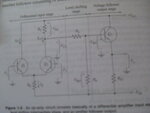
i'm sorry.here's the complete circuit.j.jpg
 

If the feedback is not acting,is the wire not doing anything?

I think the feedback being referred to is an external network that you attach to the output and inputs. The feedback can go to one or both inputs.

The simplest possible use of feedback is to connect the output to the inverting input. Negative feedback.

You can find a thousand different feedback circuits to suit the purpose you want to use the op amp for.

i read that the potentials of both the input terminals would eventually become equal.can you please explain how it happens?the book does'nt exactly explain how it happens,it merely states in words that it happens.no equations at all.

Generally your feedback circuit is designed so that the output will attempt to drive the inputs so they are at equal voltage.

Notice that once the inputs are equal, the output will stay wherever it is at.

This is only the most basic explanation.
 

You can find a thousand different feedback circuits to suit the purpose you want to use the op amp for.
Yes, but the intended feedback configuration has been clarified.
 

Frankly speaking, the way Q2 and Q3 are connected on the 2nd circuit creates the negative feedback and makes the circuit stable. The more current flows through Q2 collector, the less current flows into Q3 base, preventing further Q2 collector current increase and restoring the balance. This makes the output circuitry stable. The reference point is the junction of Q1 and Q2 emitters.

Now, let's imagine that initial voltage at Q1 base is at 0V. Q1 emitter will be at -0,6V, same as Q2 emitter. This will cause certain current flow through both transistors. At the same time, base of Q3 will be driven by some current (depending all the resistors), polarizing base of Q2. Any fluctuation of currents between Q2 and Q3 will trigger the above mentioned mechanism of self-balancing, making base of Q2 and output to stay at 0Vin order to keep the balance. Now, any change of Q1 base voltage will cause the change of Q2 base - emitter voltage, resulting in Q2 collector current change (opposite to Q1), which will cause Q3 to restore balance at the level defined by voltage at Q1 base... So the output voltage will FOLLOW the voltage at Q1 base. The common emitter resitor of Q1 and Q2 forces them to react to each other's parameter change (voltage, current, temperature).

Excuse my language, which is not native.
 
Now, any change of Q1 base voltage will cause the change of Q2 base - emitter voltage, resulting in Q2 collector current change (opposite to Q1), which will cause Q3 to restore balance at the level defined by voltage at Q1 base...

Yes, this describes the current mirror effect which is used in the differential amp section. (And which is yet another type of feedback that goes on in or around an op amp.)

Excuse my language, which is not native.

Your explanation is helpful and you get positive feedback.

Sure looks like there's all kinds of feedback going on in this thread.
 

Frankly speaking, the way Q2 and Q3 are connected on the 2nd circuit creates the negative feedback and makes the circuit stable. The more current flows through Q2 collector, the less current flows into Q3 base, preventing further Q2 collector current increase and restoring the balance. This makes the output circuitry stable. The reference point is the junction of Q1 and Q2 emitters.

Now, let's imagine that initial voltage at Q1 base is at 0V. Q1 emitter will be at -0,6V, same as Q2 emitter. This will cause certain current flow through both transistors. At the same time, base of Q3 will be driven by some current (depending all the resistors), polarizing base of Q2. Any fluctuation of currents between Q2 and Q3 will trigger the above mentioned mechanism of self-balancing, making base of Q2 and output to stay at 0Vin order to keep the balance. Now, any change of Q1 base voltage will cause the change of Q2 base - emitter voltage, resulting in Q2 collector current change (opposite to Q1), which will cause Q3 to restore balance at the level defined by voltage at Q1 base... So the output voltage will FOLLOW the voltage at Q1 base. The common emitter resitor of Q1 and Q2 forces them to react to each other's parameter change (voltage, current, temperature).

Excuse my language, which is not native.

thank you,that was really helpful.it clearly explains the mechanism.it would be really good if you can add a few equations.thank you again.
 

Status
Not open for further replies.

Similar threads

Part and Inventory Search

Welcome to EDABoard.com

Sponsor

Back
Top