Continue to Site

Welcome to EDAboard.com

Welcome to our site! EDAboard.com is an international Electronics Discussion Forum focused on EDA software, circuits, schematics, books, theory, papers, asic, pld, 8051, DSP, Network, RF, Analog Design, PCB, Service Manuals... and a whole lot more! To participate you need to register. Registration is free. Click here to register now.

opamp circuit with MCU

Status
Not open for further replies.

omid2006

Junior Member level 1
Joined
Apr 24, 2019
Messages
17
Helped
0
Reputation
0
Reaction score
4
Trophy points
1
Activity points
89
Hi friends
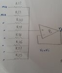
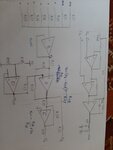
I have faced an unfamiliar opamp circuit that I'll attach its diagram too. It's a unit gain opamp circuit who connected to the common node resistors that other side of resistors connected to the microcontroller pins. It's a test equipment and I don't know what's the function of this configuration.
 

Attachments

  • photo_2020-12-27_11-15-19.jpg
    photo_2020-12-27_11-15-19.jpg
    68.9 KB · Views: 164

Hi,

Without resistor values we can just guess...
I'd say it's a "hand made" DAC.

Klaus
 

    omid2006

    Points: 2
    Helpful Answer Positive Rating
this equipment has a capacitance measurement concept so it can be true.
the value of the resistors are:
R22=31ohms
R21=68ohms
R20=39ohms
R19=10ohms
R18=62kohms
R26=31.6Kohms
R27=15.8Kohms
R25=7.87Kohms
 

Hi,

R22 ... R19 makes no sense to me
R18 .. R25 are classical 2:1 binary stages

Klaus
 

    omid2006

    Points: 2
    Helpful Answer Positive Rating
It is a digital to analog converter. A binary number on the MCU pins is converted to an analog voltage where all the resistors meet and the op-amp is to buffer the output.

It should ideally have a load resistor and some feedback but it will work as it is. Note the values of the resistors is approximately doubling although I would have expected R22 to be 22 Ohms, this is to reflect the weighting of the binary levels at the MCU pins. Maybe the lower values are 'adjusted' to correct non-linearity elsewhere.

Brian.
 

    omid2006

    Points: 2
    Helpful Answer Positive Rating
Instead of reading a sense into the posted resistor values, consider that some values have been decoded incorrectly.
 

    omid2006

    Points: 2
    Helpful Answer Positive Rating
I saw the resistors with a magnifier again.
The corrected values are:
R22=1Mohms
R21=499Kohms
R20=249Kohms
R19=124Kohms
R18=62Kohms
R26=31.6Kohms
R27=15.8Kohms
R25=7.87Kohms
Now it makes sense for you
The only remain problem for me is that its output is connected to the output of an analog mux. If you can explain to me why?
I'll attach the full diagram and consider that it's principle is to inject a signal and receive its response to evaluate the capacitance between probes.
 

Attachments

  • 16090652662011131306766855233344.jpg
    16090652662011131306766855233344.jpg
    1.3 MB · Views: 161

It is a digital to analog converter. A binary number on the MCU pins is converted to an analog voltage where all the resistors meet and the op-amp is to buffer the output.

It should ideally have a load resistor and some feedback but it will work as it is. Note the values of the resistors is approximately doubling although I would have expected R22 to be 22 Ohms, this is to reflect the weighting of the binary levels at the MCU pins. Maybe the lower values are 'adjusted' to correct non-linearity elsewhere.

Brian.
yes sir
I have corrected the resistor values in next my next post
Thanks alot
 

I don't recognize an analog mux in your schematic. Which nodes have external connections, e.g. "probes".

1609072326116.png
 

Da and Db are outputs of dg9409(analog mux)
It's inputs are the probes
What's the application of analog mux here?
View attachment 166616
[/QUOTE]
 

Hi,

I can't find an analog MUX either, nor a DG9409

Klaus
 

B and D are buffers. A is a difference amplifier. C is an inverting amplifier.
--- Updated ---

Why R34?
--- Updated ---

With the formula you wrote for A to hold, R31 = R28 and R32 = R29.
 
Last edited:

B and D are buffers. A is a difference amplifier. C is an inverting amplifier.
--- Updated ---

Why R34?
--- Updated ---

With the formula you wrote for A to hold, R31 = R28 and R32 = R29.
Da and Db connwcted to another ic
Analog mux
Its not complete circuit
 

Okay.

What do you intend to achieve with B?
It's for better loading elimination on the microcontroller
If we connect the common node of resistors to the r32, because of R31 we have a little loading effect. And this has 4 opamps so it's better to use one of them as a buffer instead of taking it away
--- Updated ---

Is your schematic correct ?


View attachment 166619

Because you are not operating into a summing junction I don't think you have a DAC -

View attachment 166625


Regards, Dana.
Thanks for your attention my friend
But it's working too
Why?
Let's assume that you have a 5v logic level. now you want to build 5/3v on the output of your handmade DAC
With your adder config, you can put 0100 on the digital inputs if R3=3k
But with my config, I can put Vd=5v and Vc=gnd and float for others
 
Last edited:

I'm just wondering what v+ of A would be if the voltage level from the MCU pins are the same, assuming the current going into the noninverting input is 0A.
--- Updated ---

Okay, I get it. The inputs form a voltage divider depending on the weight of the resistors and the voltage level at each input.
--- Updated ---

What's the of your V+ supply and what are the values of R37 and R40?
 
Last edited:

Status
Not open for further replies.

Similar threads

Part and Inventory Search

Welcome to EDABoard.com

Sponsor

Back
Top