sykab
Member level 2
Hi!
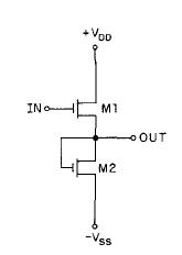
I'm designing an opamp with a differential pair. I added a second stage (common-souce amplifier) and I'm thinking that I need a third stege (source-follower).
The problem his that I have no idea how to dimension the third stage. I know that it should have a low output resistance (but between which values?).
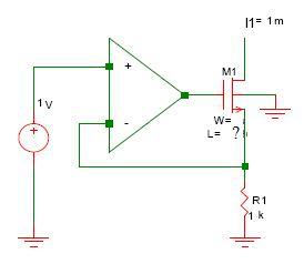
When I test if the opamp output follows the input changes (doing a vin sweep), I realise that the Resistance Voltage can follow the input sweep just when Vi is between 0 and 0,200 V. Then it (VR) keeps its value in 0,2 V.
Outside the opamp I have some elements, as you can see in the image.
Can anyonde help me?
Should the problem be outside or inside the opamp?
I'm designing an opamp with a differential pair. I added a second stage (common-souce amplifier) and I'm thinking that I need a third stege (source-follower).
The problem his that I have no idea how to dimension the third stage. I know that it should have a low output resistance (but between which values?).
When I test if the opamp output follows the input changes (doing a vin sweep), I realise that the Resistance Voltage can follow the input sweep just when Vi is between 0 and 0,200 V. Then it (VR) keeps its value in 0,2 V.
Outside the opamp I have some elements, as you can see in the image.
Can anyonde help me?
Should the problem be outside or inside the opamp?