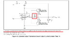
Continue to Site

Welcome to EDAboard.com

Welcome to our site! EDAboard.com is an international Electronics Discussion Forum focused on EDA software, circuits, schematics, books, theory, papers, asic, pld, 8051, DSP, Network, RF, Analog Design, PCB, Service Manuals... and a whole lot more! To participate you need to register. Registration is free. Click here to register now.

OPA454 shows clipping and odd distortion

Status
Not open for further replies.

Plecto

Full Member level 5
Joined
Jan 4, 2012
Messages
315
Helped
1
Reputation
2
Reaction score
1
Trophy points
1,298
Activity points
4,979


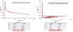
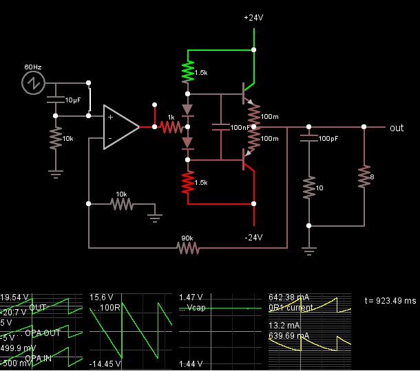
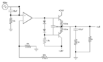
Scoping the op-amp output with a 1khz sine input signal. The supply is shown in blue (25-26V with a couple of volts of ripple):


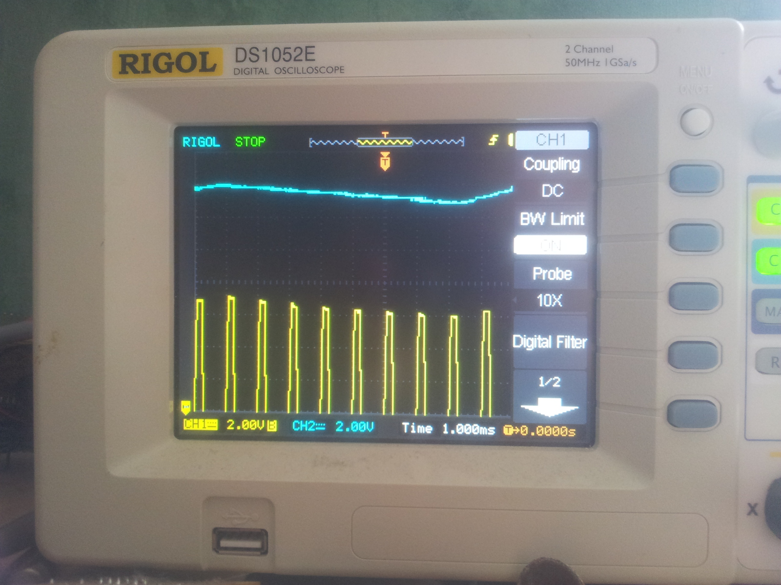
Scoping the op-amp output with a 20hz sine input signal:


The tests are done without load connected. The OPA454 is supposed to output about 1V close to the rails, but it starts clipping 6-7V from the rail. When testing with a 20hz signal the op-amp starts doing some odd distortions even sooner (8V from the rails). I have a 10Ohm shunt to be able to measure the actual current output of the op-amp, but it measures to about 4-5mA which is expected and no where near being current starved. The op-amp should be able to output about +/-24V shouldn't it?
 
Last edited by a moderator:

The gain selector is on 68K that gives gain of about 2.5, if your signal input is 5V you wont get 25V output. Switch the selector to 4.2K.
 

  • Open loop output impedance of OPA is very high, especially at 20Hz
  • Although it is reduced significantly by feedback ratio. (Aol/Acl) Thus raising the Acl gain will also raise the source impedance.
  • The MJE3055 has high output current but a wide tolerance on hFE which means input impedance is limited by hFE*Re +240+10Ω, where Re=0.1
  • Lower the gain selector R value will increase gain but also output impedance.
  • I am not familiar with this chip, but it does not seem to be working as expected.
  • Replace MJE's with a 2K load R for testing then 1K. Drive full scale and Note the drop from rail and compare vs f. 20Hz to 20KHz
  • Also consider other parts.


OPA547 60V, 750mA
OPA548 60V, 3A
OPA549 60V, 9A
OPA551 60V, 200mA

I assume E/D COM = 0V gnd.
 

Since the transistors are not powered then the poor opamp has no negative feedback and is clipping like crazy.
 

A pair of equal value resistors should be connected across C1 and C2 so as to stabilise the earth to be a half of the +Vcc and -Vcc. Try 100 ohms, its value will depend on the currents in the respective voltage lines.
Frank
 

A pair of equal value resistors should be connected across C1 and C2 so as to stabilise the earth to be a half of the +Vcc and -Vcc. Try 100 ohms, its value will depend on the currents in the respective voltage lines.
Frank
Since the transformer has a center-tap then the resistors are not needed.
 

Since the transistors are not powered then the poor opamp has no negative feedback and is clipping like crazy.

If there is no power connections to the transistors and also no load (as OP) then there will be no clipping and no distortion at all, only 0.6V lost on the Vbe of the transistors.
 

The digital 'scope seems to have a very low sampling frequency and is chopping up the waveform. The waveform is odd that it does not show a negative swing nor 0V and shows only the most positive part.
 

Sorry for not getting back to this thread sooner. The transistors are connected to +V and -V, there's just an error in the schematic, I'm sorry about that.

I am measuring the output of the op-amp itself, not the output of the amplifier (between the 0.1Ohm resistors).

The digital 'scope seems to have a very low sampling frequency and is chopping up the waveform. The waveform is odd that it does not show a negative swing nor 0V and shows only the most positive part.

I did this to accurately measure the difference in voltage between the op-amp output and the positive rail. The resolution of the screen isn't big enough to give me any usable information if it were to show both positive and negative swing.

Open loop output impedance of OPA is very high, especially at 20Hz
Although it is reduced significantly by feedback ratio. (Aol/Acl) Thus raising the Acl gain will also raise the source impedance.
The MJE3055 has high output current but a wide tolerance on hFE which means input impedance is limited by hFE*Re +240+10Ω, where Re=0.1
Lower the gain selector R value will increase gain but also output impedance.
I am not familiar with this chip, but it does not seem to be working as expected.
Replace MJE's with a 2K load R for testing then 1K. Drive full scale and Note the drop from rail and compare vs f. 20Hz to 20KHz
Also consider other parts.

I will try to remove the output stage all together to see if the OPA454 can manage a higher swing without any load at all. Is there a reason to think that the OPA454 isn't fit for the task in this application? Maximum output current is only about 1A.
 

I fixed your schematic.
I think the resistors that bias the output transistors have them almost in class-A with fairly high current between them. Their current will increase as they warm up. Then their base current is delivered from the opamp instead of from the bias resistors and the opamp is overloaded even when the amplifier has no load. Diodes (or a transistor) should have been used instead to better match the base emitter junctions of the output transistors and they can also match temperature changes.
 

Attachments

  • amplifier with opamp.png
    amplifier with opamp.png
    198.1 KB · Views: 134

Thank you, that looks a lot better :)

The amplifier is biased well into class A, but that's also the point. I know that the op-amp will deliver the current, but that's why I chose a high-current op-amp. The 10Ohm resistor shown in the schematic is a current sense resistor and it only shows 4-5mA at maximum output swing (which is expected giving the 6.8k resistors that will act as a load), the op-amp should be able to output 50mA though so I'm well within it's limits. I know that biasing diodes would have been a better idea, but I don't know how to do that. Replacing the 240 Ohm resistors with diodes will prevent the op-amp from supplying base current thus massively hinder the output voltage swing of the amplifier.
 

Don't you understand that almost ALL audio amplifiers use diodes (or a transistor acting like two diodes) replacing your 240 ohm resistors to bias the output transistors in class-AB? The diodes or extra transistor have exactly the same temperature coefficient as the output transistors when mounted on their heatsink so the idle current in the output transistors remains low even when the output transistors get hot.

Your opamp is driving two turned on transistors that are "fighting" each other almost in class-A, with a current between them of almost 2A when cold and much more current when hot. The output transistors have "thermal runaway". They turn on more and more as they get hot from the current then their bases draw even more current swing from the opamp. The 6.8k bias resistor value is much too high for it to drive each output transistor to its maximum voltage swing.

Most audio amplifiers and opamps use driver transistors to supply enough base current to the output transistors.
 

Is there any reason why you don't want to use the recommended configuration for higher current in the data sheet?

Furthermore, make sure you have E/D and E/com not causing problems as mentioned in a previous posting.
 

Attachments

  • opa454.png
    opa454.png
    32.1 KB · Views: 122

The transistors doesn't go thermal runaway, the collector current is about 150mA when cold and about 200mA when heated to about 70C. I've made several of these amplifier and the bias current is very reliable and I've never experienced the current rising more than 50% as the transistors heat up in a predictable fashion.

How can maximum output voltage be reached when this biasing configuration is used:?

**broken link removed**

The output voltage swing will be limited by 0.6+ib*R so unless I choose resistor values down in the hundreds this will severely limit output voltage. Using a transistor to supply the base current seems interesting though, do you have an example schematic I can look at?

Is there any reason why you don't want to use the recommended configuration for higher current in the data sheet?

I did look at that, but I do wan't this amplifier to be fully class A, I need to warm my fingers during winter. I also can't see how that configuration won't add crossover distortion as the gain between 0.7V and -0.7V will be less than during the rest of the swing, right?
 

I did look at that, but I do wan't this amplifier to be fully class A, I need to warm my fingers during winter. I also can't see how that configuration won't add crossover distortion as the gain between 0.7V and -0.7V will be less than during the rest of the swing, right?

They don't produce data sheets and app notes because they have nothing better to do. Below you can see that simulation results show superior performance using the configuration in the data sheet.
 

Attachments

  • opa454_dist.png
    opa454_dist.png
    31.4 KB · Views: 100

How are you measuring OPA output current? twin probe in diff mode? (A-B)

Simplified design, with critical details not shown;
- diode selection or adding ESR and high matching hFE in Q1,2,, thermal coupling diodes to Q

5130924000_1429549394.jpg


Next figure why cct gain is 40x here with OTA gain of 10
 

I would simplify the circuit by letting the output of the opamp run in class-A maybe reducing its distortion (but reducing the maximum output level a little).
 

Attachments

  • amplifier.png
    amplifier.png
    22.9 KB · Views: 148

How are you measuring OPA output current? twin probe in diff mode? (A-B)

Simplified design, with critical details not shown;
- diode selection or adding ESR and high matching hFE in Q1,2,, thermal coupling diodes to Q

I measure the op-amp current with my DMM in AC mode.

I still struggle to see how that configuration will work. If my math is correct, output voltage swing will be limited by IL/Hfe*1500+0.6 which for a 16Ohm load will limit the output voltage of about 12V which is huge, plus I'll be needing high power biasing resistors. I know the benefits of using diodes for biasing, but having such huge limitations on the output voltage swing has to be a factor, no? What about using a zener diode with a reverse breakdown voltage of 0.6V? Or using two diodes in opposite directions so that the op-amp can in fact supply the base current?

They don't produce data sheets and app notes because they have nothing better to do. Below you can see that simulation results show superior performance using the configuration in the data sheet.

I really don't hope my amplifier has a distortion figure of 7%? If so, why?
 

Status
Not open for further replies.

Similar threads

Part and Inventory Search

Welcome to EDABoard.com

Sponsor

Back
Top