Continue to Site

Welcome to EDAboard.com

Welcome to our site! EDAboard.com is an international Electronics Discussion Forum focused on EDA software, circuits, schematics, books, theory, papers, asic, pld, 8051, DSP, Network, RF, Analog Design, PCB, Service Manuals... and a whole lot more! To participate you need to register. Registration is free. Click here to register now.

Op-amp Power Boost Discrete Stage

Status
Not open for further replies.

sesj13

Newbie level 5
Joined
Apr 22, 2013
Messages
8
Helped
0
Reputation
0
Reaction score
0
Trophy points
1,281
Activity points
1,386
Hello,

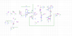
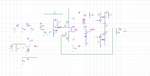
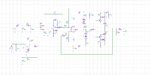
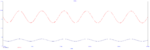
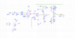
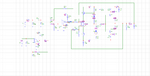
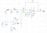
I am using a DAC which can output 0V to 3.3V and this goes into an op-amp to boost it to 0V to 10V. This is fed into a unity-gain differential amplifier which also AC-couples in a 1Vpp sinewave. The resulting signal is a 0V to 10V DC level with the sinewave superimposed on it. I need to boost this signal by amplifying its voltage gain by 5 so it is 0V to 50V DC level with a 5Vpp sinewave superimposed on it. This signal will be used to drive a capacitive load of a couple of microfarads, so adequate current gain is also required.
  1. Three voltage rails in the design: 50V, 10V, 3.3V.
  2. Amplification of DAC level and the differential amplifier are rail-to-rail op-amps supplied from 10V rail.
  3. Single supply power stage: 50V to GND.
  4. The power stage must be discrete due to costs in high-voltage op-amps.
  5. Needs to go close to rails, but a diode drop away is okay.
I have been reading the following application notes:

**broken link removed**

I would really appreciate it if you have advice regarding this design or you can recommend any application notes. Thanks.
 

Attachments

  • Opamp-1.PNG
    Opamp-1.PNG
    32.1 KB · Views: 89
  • Opamp-2.PNG
    Opamp-2.PNG
    16 KB · Views: 93
  • Opamp-3.PNG
    Opamp-3.PNG
    5.6 KB · Views: 95

you don't give any mention of frequency. I might think that's an important piece of information.
 

    sesj13

    Points: 2
    Helpful Answer Positive Rating
Sometimes you only need to mix two signals rather than use an op amp (differential amplifier).
I have a hunch a class A transistor amplifier is sufficient. Power it from 50VDC. With experimentation it should be possible to find the right combination of bias network and bias voltages. (Example, one potentiometer selects middle point between your input signals, another potentiometer selects bias voltage.)

I can see it's a question whether the transistor should be PNP or NPN. It depends on which creates voltage swings as high as the 50V rail.
 

    sesj13

    Points: 2
    Helpful Answer Positive Rating
Hi,

Your specifications are inconsistent.
For example:
* you can't amplify a 0V...10V signal by 5 ...while the amplifier is powered by 0V..50V.

There are several problems
* no Opamp will go exactly to the rail...just close to it --> signal will be clipped
* with the "one diode drop" from rails you can't use gain of 5 --> signal wil be additionally clipped
* power supplies' output voltage isn't that exact. It has some tolerance. Lets say +/-2% to +/-5V. It will change with time, with load current and with temperature.
* When adding your AC signal then you need an even wider output signal range. Expect that more than half of your sine signals is clipped.
Expect "50V" with 5% tolerance to be in the range of 47.5V to 52.5V
* resistors are not ideal, thus the gain setting is not ideal. Calculate some tolerance in.

Your values are "idealized" this means they are not realistic.
Generally when you want to go close to the limits you need to expect trouble.
Like: Opamps may cause increased distortion when operated close to the rails.

So either:
* adjust your requirements
* or accept signal clipping and other effects

Klaus
 

    sesj13

    Points: 2
    Helpful Answer Positive Rating
Hello everyone,

Thank you for your replies. :) You are all correct that I have missed out some important information, so to clarify:
  1. Three voltage rails in the design: 50V, 10V, 3.3V.
  2. The DC DAC level is amplified 3x by a rail-to-rail opamp taking it from 0..3.3V to 0..10V.
  3. The rail-to-rail differential amplifier superimposes the 1Vpp sinewave onto the amplified DAC level.
  4. The sinewave will only be activated when away from the rails so clipping does not occur. This will be handled by the microcontroller.
  5. The amplified DC level needs to go close to rails, but a diode drop away is okay.
  6. The sinewave frequency is: 500Hz to 2kHz.
  7. Single supply power stage: 50V to GND.
  8. The output from the power stage will be fed back to a microcontroller so that it can adjust the DAC and sinewave peak-peak to compensate for passive tolerances and power supply tolerances.
  9. The power stage must be discrete due to costs in high-voltage op-amps.
Klaus, what do you exactly mean by "you can't amplify a 0V...10V signal by 5 ...while the amplifier is powered by 0V..50V "?

Thanks again everyone.
 

Klaus first gave the statement:, " you can't amplify a 0V...10V signal by 5 ...while the amplifier is powered by 0V..50V. "
And then provided the 5 reasons immediately afterwards.
 

Okay thanks, I understand - it was just how I read the initial post. I have amended the design requirements which hopefully address the concerns.
 

The power stage must be discrete due to costs

Going by your specifications, this transistor amplifier is a cheap way and it does a couple of jobs. Class A. NPN transistor. Power supply 50V single-ended.

Your two signals are mixed through bias resistors. Correct values are found through trial and error. Adjustments go more quickly if you use potentiometers.

two signals mixed into class A amplifier NPN 50V supply.png
 

Going by your specifications, this transistor amplifier is a cheap way and it does a couple of jobs. Class A. NPN transistor. Power supply 50V single-ended.

Your two signals are mixed through bias resistors. Correct values are found through trial and error.
I humbly, but strongly, disagree. Correct values are found by design. If circuit tolerances (beta, for example) are unacceptable, then the circuit needs to have some feedback. Maybe there also needs to be some thermal compensation. But good circuit design does not involve “trial and error”.
 

Thank you for your replies. :) You are all correct that I have missed out some important information, so to clarify:
  1. Three voltage rails in the design: 50V, 10V, 3.3V.
  2. The DC DAC level is amplified 3x by a rail-to-rail opamp taking it from 0..3.3V to 0..10V.
  3. The rail-to-rail differential amplifier superimposes the 1Vpp sinewave onto the amplified DAC level.
  4. The sinewave will only be activated when away from the rails so clipping does not occur. This will be handled by the microcontroller.
  5. The amplified DC level needs to go close to rails, but a diode drop away is okay.
  6. The sinewave frequency is: 500Hz to 2kHz.
  7. Single supply power stage: 50V to GND.
  8. The output from the power stage will be fed back to a microcontroller so that it can adjust the DAC and sinewave peak-peak to compensate for passive tolerances and power supply tolerances.
  9. The power stage must be discrete due to costs in high-voltage op-amps.
Detailed requirements but yet little effort to achieve it.

@5: below one diode drop saturation voltage. Only one of the linked application notes (Linear technology) is proposing a circuit with low saturation voltage. Figure 7 design could be modfied to support high unipolar supply.

1593865676070.png

@9: There are a lot of economic medium voltage (60 - 100V) power amplifiers which promise less overall costs than a discrete design. Low saturation voltage requirement may be a problem though.

A previous requirement has been omitted in your latest post, although it's critical too: "This signal will be used to drive a capacitive load of a couple of microfarads". Loop compensation must be adjusted respectively.
 

Hello all,

Thank you for taking the time to reply to this thread. This is quite a tricky problem (at least for me), so I have been busy reading and educating myself. I do not think I have the knowledge to design a purely-discrete stage, however, after reading **broken link removed** article, I have been toying with the idea of using a 30V opamp (which are a lot more common than >50V opamps).

I simulated a circuit based on this concept and it looks like it could work, I have also added a push-pull stage to drive the capacitive load. I have added a -3.3V rail to ensure that the inputs to X3 stay within their rails when driving down to 0V. I had considered the AD820 as it allows the inputs to be driven far below the negative rail, however, it is quite expensive. There looks to be some oscillation on the output which can be seen in "Driver-5.png". General thoughts on the circuit?

Thanks.
 

Attachments

  • Driver-1.png
    Driver-1.png
    81 KB · Views: 91
  • Driver-2.png
    Driver-2.png
    64.3 KB · Views: 98
  • Driver-3.png
    Driver-3.png
    65 KB · Views: 75
  • Driver-4.png
    Driver-4.png
    16.2 KB · Views: 89
  • Driver-5.png
    Driver-5.png
    11.9 KB · Views: 86

I can’t put my finger in the exact details, but there is something in the way you are biasing the output stage that doesn’t look right.

What is the output stage’s idle current ?
 

Hi,

As others already mentioned: There is no need for the first Opamp stage, there is no need fo a differential Opamp circuit.
But it's no mistake, either.
But if you want it to ve a true differential srage, then do it correctly:
* value of R9 = value of R8.
* if you place a capacitor across R8, then also place the same value capacitor across R9.

R5 may be omitted.

I don't understand the positive feedback via R12. What happens if you omit it?
To stabilize the circuit, I'd put a small capacitor from X3_out to X3_InvIn.
Treat X3 as simple non inverting Opamp stage

I doubt the otput stage is able to actively drive close to the rails as required. What does the simulation show in this regard?

Why are the Opamps named with "X"?

Klaus
 

You are requiring voltage swing to supply voltage minus one diode drop (post #1, #6) but your post #12 circuit that has at least several volts saturation voltage. An off-the-shelf integrated audio power amplifier will probably achieve better performance.
 

Hello all,

Thanks for your replies, it is appreciated. To answer your questions:
  1. The output stage’s quiescent currents can be seen in the attached, “Driver-6.png”.
  2. The output is able to drive up to ~48.3V and down to ~0V thanks to the addition of the -3V3 rail. Does anyone have any thoughts on how this could be improved?
  3. The positive feedback via R12 helps keep the inputs within the op-amp's input common-mode range. See, “Driver-7.png” with R12 removed and R11 / R13 adjusted to give the same gain.
  4. I have considered off-the-shelf op-amps. However, they are expensive and I wouldn’t learn nearly as much.
  5. The op-amps are labeled “X” because that is what Micro-cap uses as a default designator.
  6. I will see if I can tidy up the circuit and remove one of the op-amps.
Thanks again.
 

Attachments

  • Driver-6.png
    Driver-6.png
    86.2 KB · Views: 86
  • Driver-7.png
    Driver-7.png
    63.9 KB · Views: 75

Status
Not open for further replies.

Similar threads

Part and Inventory Search

Welcome to EDABoard.com

Sponsor

Back
Top