Continue to Site

Welcome to EDAboard.com

Welcome to our site! EDAboard.com is an international Electronics Discussion Forum focused on EDA software, circuits, schematics, books, theory, papers, asic, pld, 8051, DSP, Network, RF, Analog Design, PCB, Service Manuals... and a whole lot more! To participate you need to register. Registration is free. Click here to register now.

Op Amp Design - Hand Calc Questions

Status
Not open for further replies.

terranpro

Newbie level 4
Joined
Mar 1, 2009
Messages
5
Helped
0
Reputation
0
Reaction score
0
Trophy points
1,281
Activity points
1,324
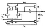
Trying to follow the example in Allen's book for a two stage op-amp design (6.3)

Could someone explain the constraints placed on the common mode input range?

Vin_max = VDD - sqrt(I5/beta3) - |VT03max| + VT1min

Vin_min = VSS + sqrt(I5/beta1) + |VT1max| +VDS5(sat)

I don't understand his terminology, what is VT03max, and what is VT1min and max?

I tried to derive these on my own by writing the large signal Id (saturation) equations, and keeping the constrains (Vds versus Vgs-Vt) satisfied; is this the right approach?

Also, If I have an output swing range limitation, how/where do I consider that?

i would appreciate as much explanation as possible (i am a beginning analog ic student) - thanks
 

Attachments

  • twostage_opamp.jpg
    twostage_opamp.jpg
    23.4 KB · Views: 149

I not sure exactly, but perhaps keep in mind definition of Vt (eg. section 3.1), Vt = Vt0 + f(Vsb), a function of source-bulk voltage. So VT03 refers to threshold voltage of M3 which has source-bulk connected (so Vt == Vt0), whereas M1 hasn't got bulk-source connected and so Vt1 depends on Vin.

Yes, large signal Ids equation and Vds>=(Vgs-Vt) is the right approach.

To consider output range - see what limits output voltage. With two-stage op-amp second stage can swing to both positive and negative rails, but distortion results if you get within one Vdsat of Vdd or Vss and M6/7 go out of saturation (so gain of the overall op-amp decreases), it depends on the application whether this is a problem. Maybe swing on output of first stage should also be considered, although as the swing here is the output swing divided by the gain of the second stage, swing here will be quite small.
 
"I tried to derive these on my own by writing the large signal Id (saturation) equations, and keeping the constrains (Vds versus Vgs-Vt) satisfied; is this the right approach?"

This approach is not necessary.
The easy way is just to remember, for analog design ,each MOS must be in saturation region,so you need to make Vds>Vds(sat).

For ex, in terms of Vmin, you need to keep M5 in sat region.so Vin-Vgs1-Vss>Vds5(sat), and just remember for Vgs1=Vt+sqrt(2I/beta),and you can get the right answer.The same approach can be used to derive Vmax to make sure M1 is in sat region.
 
Status
Not open for further replies.

Similar threads

Part and Inventory Search

Welcome to EDABoard.com

Sponsor

Back
Top