masab_ahmad
Member level 1
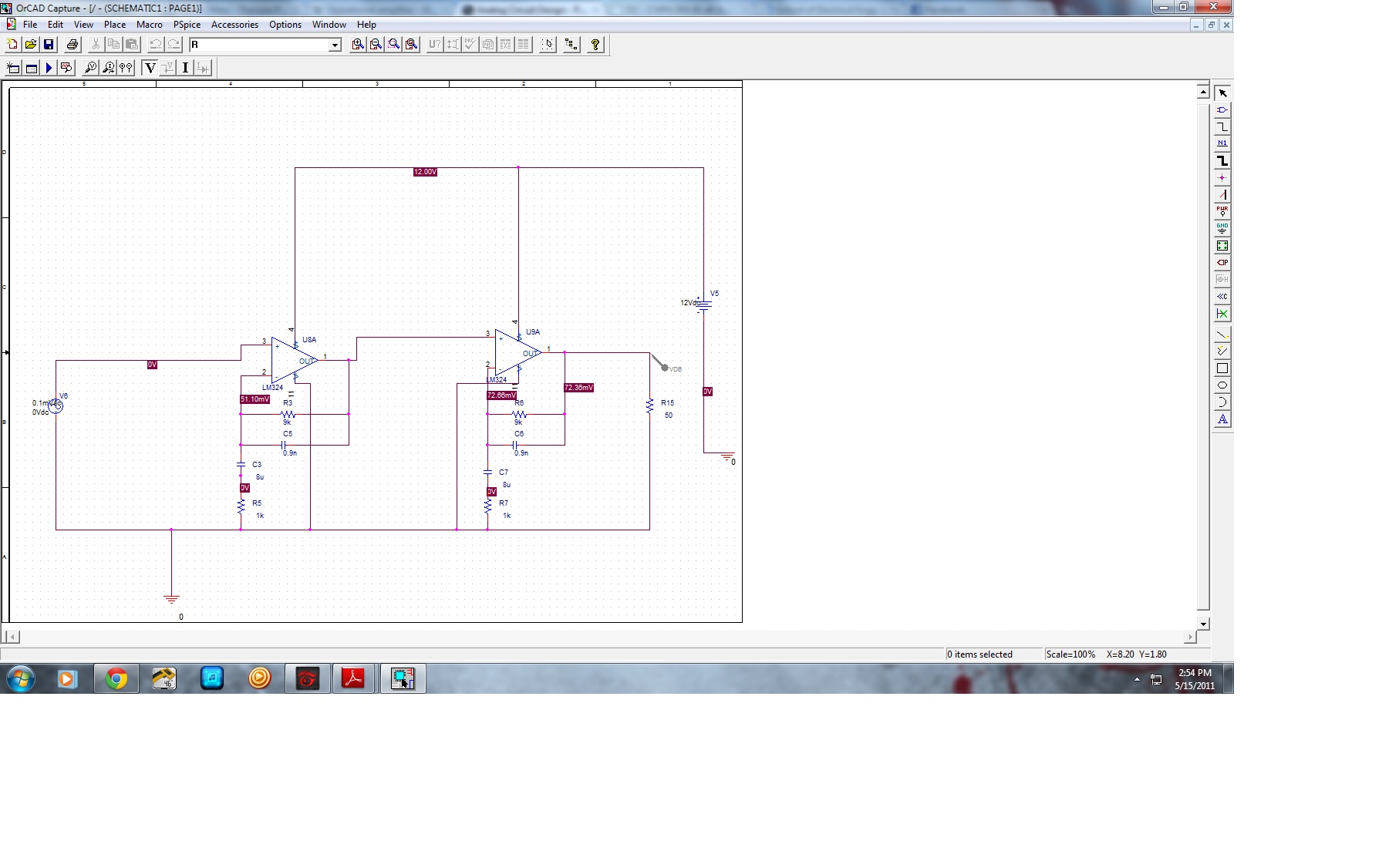
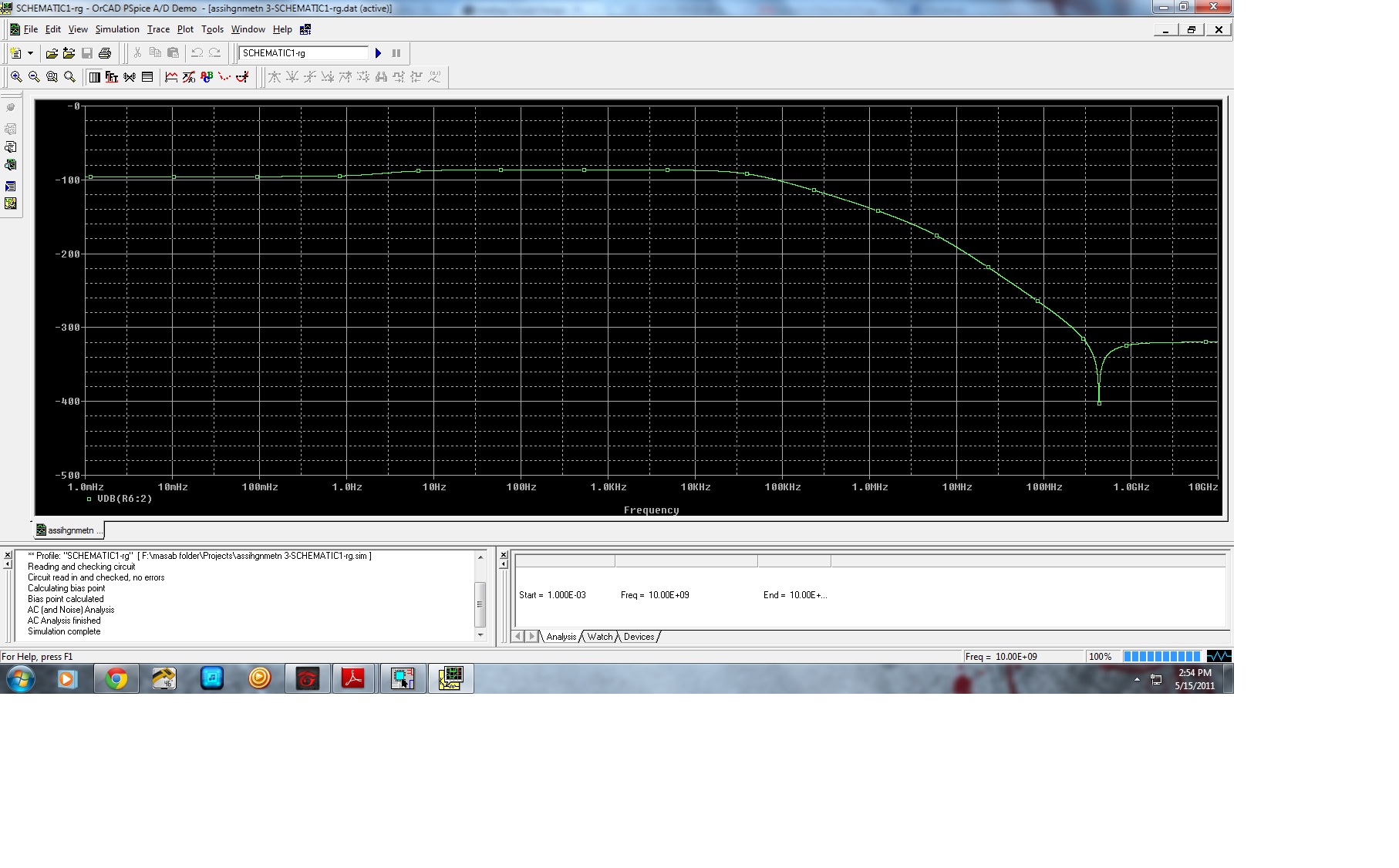
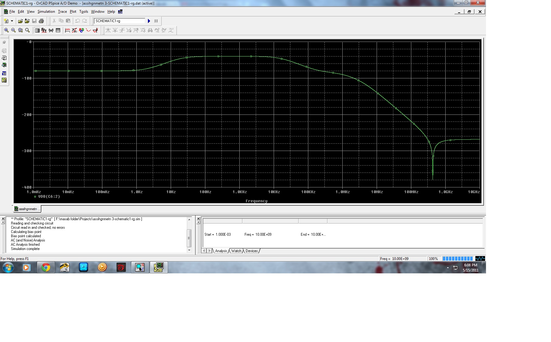
how to get an op amp circuit working with the following considerations in PSPICE:
1. Gain = 40dB
2. Bandwidth = 20Hz to 20KHz
3. The frequency response should have +40dB and -40dB slope for the corners of the bandwidth.
4. Assume a load of 50Ω.
5. Assume a sinusoidal input of 100uV amplitude.
i do get the first 4 options done at 1V ac with a 1V dc offset, but when i adjust to the 5th option the circuit doesnt give any gain..plz help
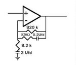
pics:
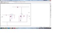
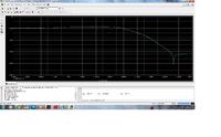
1. Gain = 40dB
2. Bandwidth = 20Hz to 20KHz
3. The frequency response should have +40dB and -40dB slope for the corners of the bandwidth.
4. Assume a load of 50Ω.
5. Assume a sinusoidal input of 100uV amplitude.
i do get the first 4 options done at 1V ac with a 1V dc offset, but when i adjust to the 5th option the circuit doesnt give any gain..plz help
pics: