chandra3789
Member level 1
I simulated 10 bit pipelined ADC with 1.5bit/stage architecture with ideal blocks and now want to move on to its transistor level implementation...while simulating it with ideal blocks i got some basic doubts......please clarify them
1) i am using 0.18um cmos9t5v technology....
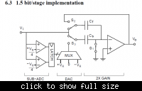
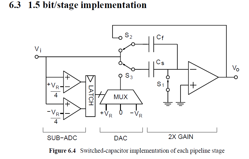
in 1.5 bit stage architecture as shown below we need two comparators one with positive VRef/4 and the other with -VRef/4 thresholds and
my input signal can range from -vref to +vref which means i can give a double polarity(both +ve and -ve) signal as input...
hence if u want to pass a signal which has two polarities your op amp which u use in S/H circuit should allow to pass them which means that the op amp has to have power supplies -0.9V and +0.9V.....
because if we use 0 and 1.8V supplies the ICMR of the op amp would be positive somewhere symmetric about 900mV and hence it cannot pass negative signals!......
one more doubt which makes my above question strong is since the residue we pass from one stage to the next can be positive or negative the op amp must be able to give negative as its output which means that op amp must have two supplies +0.9V and -0.9V but in almost all the publications i saw they showed op amps driven by 1.8V and gnd!....
so my question is should i use two polarity supplies or single supply for all the blocks i will be designing?.....i am really in confusion please help me......
2) if we use differential implementation should i go for differential op amp design or single ended one?
1) i am using 0.18um cmos9t5v technology....
in 1.5 bit stage architecture as shown below we need two comparators one with positive VRef/4 and the other with -VRef/4 thresholds and
my input signal can range from -vref to +vref which means i can give a double polarity(both +ve and -ve) signal as input...
hence if u want to pass a signal which has two polarities your op amp which u use in S/H circuit should allow to pass them which means that the op amp has to have power supplies -0.9V and +0.9V.....
because if we use 0 and 1.8V supplies the ICMR of the op amp would be positive somewhere symmetric about 900mV and hence it cannot pass negative signals!......
one more doubt which makes my above question strong is since the residue we pass from one stage to the next can be positive or negative the op amp must be able to give negative as its output which means that op amp must have two supplies +0.9V and -0.9V but in almost all the publications i saw they showed op amps driven by 1.8V and gnd!....
so my question is should i use two polarity supplies or single supply for all the blocks i will be designing?.....i am really in confusion please help me......
2) if we use differential implementation should i go for differential op amp design or single ended one?
