Continue to Site

Welcome to EDAboard.com

Welcome to our site! EDAboard.com is an international Electronics Discussion Forum focused on EDA software, circuits, schematics, books, theory, papers, asic, pld, 8051, DSP, Network, RF, Analog Design, PCB, Service Manuals... and a whole lot more! To participate you need to register. Registration is free. Click here to register now.

Omnidirectional Planar Microstrip Antenna with ADS

Status
Not open for further replies.

savvasha

Newbie level 4
Joined
Mar 3, 2008
Messages
5
Helped
0
Reputation
0
Reaction score
0
Trophy points
1,281
Activity points
1,326
Hello there. I am trying to design on ADS the antenna mentioned on the title. I am having some problems though. Ah, I forgot to mention that I am trying to design the antenna that is mentioned at https://ieeexplore.ieee.org/iel5/8/29739/01353517.pdf.

My problems are the following:
(a) I am using a board with two metal layers, top and botto. How can I define that with the substrate editor on Momentum? I am attaching my current configuration. Is it right?

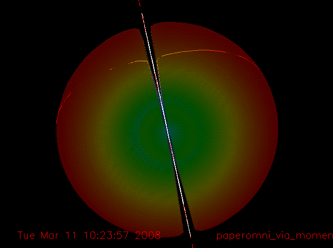
(b) I have to add two shorts on the design. I am using the command "VIA" but I am not sure what to change at the dialogue window. I am attaching the window also. My top layer is cond2 and bottom cond

(c) While simulating, the program complains that the port is internal. How that can affect my results?

Thanks in advance and sorry for my bad english :)
 

hi,
1- sorry the configuration you are mention it is not correct, you need to remove the ground, select it and chose open boundary. and there is no need for the Free space layers.

2- the via is correct for the short option in one condition it should be between the two layers metal you are using for antenna.

3-the internal port will not affect you accuracy, it is simply says that the feeding point is not at the edge of the conductor, but I believe you should use differential port.

if you want me to check it please update the project and I will check it.

hope that I helped you.
 

Thank you for your reply.

1) If I remove the ground and the second freespace layer, how am I suppose to define the two metal layers? (cond2-top and cond-bottom)

2) So at the HoleLayer="I will put the substrate?"

3) I have already use differential port :)

I will try them when I will be back home and I will send you my project.

THANKS!

Added after 4 hours 32 minutes:

Hi again. I am attaching the project to check it out. I still cant find how to setup the substrate so as at the top of the substrate there will be the layer cond2 and at the bottom of the substrate the layer cond.

Thanks in advance,
Savvas
 

Hi,
The substrate is correct.

the feeding point is not correct !! not similar to the paper.

Sorry I was busy.

I will try to simulate it, if time allows soon.

Added after 2 hours 9 minutes:

Hi,

I believe that the inaccuracy in the simulation is due to the fact that the substrate(Comclad) is not finite in the Momentum. Maybe that why he is using a 3D software to simulate it.
 

Hello again. What do you mean about the feeding point? The paper has it at the point that the narrow and the width section are connected. Or not?

I think that I found what it was going wrong with the vias. If I select for the HoleLayer = "hole" from the list, its seems ok!

About the substrate, I have to make it work with the ADS, unfortunately...

Anyway, thanks for your help. I hope someone else can have any more clues about this.... design :)
 

Hi,

according to the savvasha_prj the feeding point is not in it right place, I attached the project that I worked on, check paperomni_via_momentum where I moved the feeding point to the required point as mentioned in the paper. and also I used the via in the momentum, by attaching the vias layer in the stack-up check it.

the performance seems similar except for the x-z plane there is a null which causes the radiation pattern to be disturbed, this is maybe due to the fact that the substrate extends beyond the dimensions of the copper, I am not sure.

I found two web sources about this OMA antenna, maybe you have seen them but to finalize this issue, hxxp://www.centurion.com/home/pdf/wp_omni_wireless.pdf, hxxp://www.lecad.uni-lj.si/~leon/other/wlan/oma/index.html.

hoping some one will you in the design any help that I can do for you let me know.


see you
 

    savvasha

    Points: 2
    Helpful Answer Positive Rating
Thanks mate, I will give it a look :)

Thanks again :)

EDIT: So instead of using the VIA component, you just set a new layer and you define it on the substrate dialogue as via via? Clever :)
 

Status
Not open for further replies.

Part and Inventory Search

Welcome to EDABoard.com

Sponsor

Back
Top